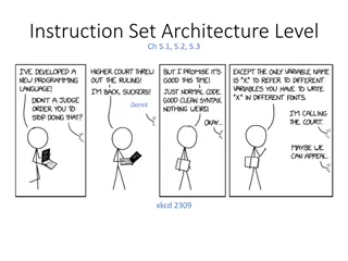
Understanding Combinational Circuits in Computer Architecture

Combinational circuits in computer architecture play a crucial role in transforming binary information from input data to output data. These circuits consist of logic gates connected in a specific arrangement to process binary data efficiently. Key components such as half-adders and full-adders are fundamental in performing arithmetic operations on binary digits. This summary covers the basics of combinational circuits, including their functioning, design, and significance in computer organization and architecture.

Download Presentation

Please find below an Image/Link to download the presentation.
The content on the website is provided AS IS for your information and personal use only. It may not be sold, licensed, or shared on other websites without obtaining consent from the author. Download presentation by click this link. If you encounter any issues during the download, it is possible that the publisher has removed the file from their server.
E N D
Presentation Transcript
Computer Architecture Part II Flip-Flops Department of Computer Science, Faculty of Science, Chiang Mai University
Outline Combinational Circuits Flips-Flops Sequential Circuits 2 204231: Computer Organization and Architecture
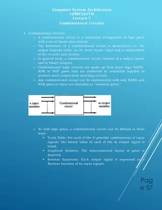
Combinational Circuits A combinational circuit is a connected arrangement of logic gates with a set of inputs and outputs. The n binary input variables come from an external source, the m binary output variables go to an external destination, and in between there is a interconnection of logic gates. A combinational circuit transforms binary information from the given input data to the required output data. 3 204231: Computer Organization and Architecture
Block Diagram of a Combinational Circuit 4 204231: Computer Organization and Architecture
Half-Adder The most basic digital arithmetic circuit is the addition of two binary digits. A combinational circuit that performs the arithmetic addition of two bits is called a half- adder. One that performs the addition of three bits (two significant its and a previous carry) is called a full- adder. The name of the former stems from the fact that two half-adders are needed to implement a full- adder. 5 204231: Computer Organization and Architecture
Half-Adder 6 204231: Computer Organization and Architecture
Half-Adder We assign symbols x and y to the two input variables, and S (for sum) and C (for carry) to the two output variables. The C output is 0 unless both inputs are 1. The S output represents the least significant bit of the sum. S = x y + xy = x y C = xy 7 204231: Computer Organization and Architecture
Full-Adder A full-adder is a combinational circuit that forms the arithmetic sum of three input bits. Two of the input variables, denoted by x and y, represent the two significant bits to be added. The third input, z, represents the carry from the previous lower significant position. The two outputs are designated by the symbols S (for sum) and C (for carry). The binary variable S gives the value of the least significant bit of the sum. The binary variable C gives the output carry. 8 204231: Computer Organization and Architecture
Truth Table for Full-Adder 9 204231: Computer Organization and Architecture
Maps for Full-Adder A variety of ways 10 204231: Computer Organization and Architecture
Full-Adder Circuit 11 204231: Computer Organization and Architecture
Flip-Flops The most common type of sequential circuit is the synchronous type. Synchronization is achieved by a timing device called a clock pulse generator that produces a periodic train of clock pulses. The clock pulses are distributed throughout the system in such a way that storage elements are affected only with the arrival of the synchronization pulse. 12 204231: Computer Organization and Architecture
Flip-Flops The storage elements employed in clocked sequential circuits are called flip-flops. A flip-flop is a binary cell capable of storing one bit of information. It has two outputs, one for normal value and one for the complement value of the bit stored in it. A flip-flop maintains a binary state until directed by a clock pulse to switch states. 13 204231: Computer Organization and Architecture
SR Flip-Flop It has three inputs, labeled S (for set), R (for reset), and C (for clock). It has an output Q and sometimes the flip-flop has a complemented output, which is indicated with a small circle at the other output terminal. There is an arrowhead-shaped symbol in front of the letter C to designate a dynamic input. The dynamic indicator symbol denotes the fact that the flip-flop responds to a positive transition (from 0 to 1) of the input clock signal. 14 204231: Computer Organization and Architecture
SR Flip-Flop If there is no signal at the clock input C, the output of the circuit cannot change irrespective of the values at inputs S and R. Only when the clock signal changes from 0 to 1 can the output be affected according o the values in inputs S and R. 15 204231: Computer Organization and Architecture
SR (Set-Reset) Flip-Flop 16 204231: Computer Organization and Architecture
D Flip-Flop The next state Q(t + 1) is determined from the D input. A D flip-flop has the advantage of having only one input (excluding C). It has disadvantage that its characteristic table does not have a no change condition Q(t + 1) = O(t). The no change condition can be accomplished either by disabling the clock signal or by feeding the output back into the input, so that clock pulses keep the state of the flip-flop unchanged. 17 204231: Computer Organization and Architecture
D (Data) Flip-Flop Q(t + 1) = D 18 204231: Computer Organization and Architecture
JK Flip-Flop Inputs J and K behave like inputs S and R to set and clear the flip-flop, respectively. When inputs J and K are both equal to 1, a clock transition switches the outputs of the flip-flop to their complement state. 19 204231: Computer Organization and Architecture
JK Flip-Flop 20 204231: Computer Organization and Architecture
T Flip-Flop The T flip-flop has only two conditions. When T = 0 (J = K = 0) a clock transition does not change the state of the flip-flop. When T = 1 (J = K = 1) a clock transition complements the state of the flip-flop. 21 204231: Computer Organization and Architecture
T (Toggle) Flip-Flop Q(t + 1) = Q(t) T 22 204231: Computer Organization and Architecture
Edge-Triggered Flip-Flops In this type of flip-flop, output transitions occur at a specific level of the clock pulse. When the pulse input level exceeds this threshold level, the inputs are locked out so that the flip-flop is unresponsive to further changes in inputs until the clock pulse returns to 0 and another pulse occurs. 23 204231: Computer Organization and Architecture
Positive-Edge-Triggered D Flip-Flop The value in the D is transferred to the Q output when the clock makes a positive transition. The output cannot change when the clock is in the 1 level, in the 0 level, or in a transition from the 1 level to the 0 level. 24 204231: Computer Organization and Architecture
Negative-Edge-Triggered D Flip-Flop The graphic symbol includes a negation small circle in front of the dynamic indicator at the C input. This denotes a negative-edge-triggered behavior. In this case the flip-flop responds to a transition from the 1 level to the 0 level of the clock signal. 25 204231: Computer Organization and Architecture
Edge-Triggered D Flip-Flops 26 204231: Computer Organization and Architecture
Excitation Tables The characteristic tables of flip-flops specify the next state when the inputs and the present state are known. During the design of sequential circuits we usually know the required transition from present state to next date and wish to find the flip-flop input conditions that will cause the required transition. 27 204231: Computer Organization and Architecture
Excitation Table for 4 Flip-Flops 28 204231: Computer Organization and Architecture
Excitation Tables The symbol x in the tables represents a don t- care condition. For example, in a JK flip-flop, a transition from present state of 0 to a next state of 0 can be achieved by having inputs J and K equal to 0 (to obtain no change) or by letting J=0 and K=1 to clear the flip-flop (although it is already cleared). 29 204231: Computer Organization and Architecture
Sequential Circuits A sequential circuit is an interconnection of flip-flop and gates. It consists of a combinational circuit and a number of clocked flip-flops. In general, any number or type of flip-flops may be included. 30 204231: Computer Organization and Architecture
Block Diagram of a Clocked Synchronous Sequential Circuit 31 204231: Computer Organization and Architecture
Example of a Sequential Circuit 32 204231: Computer Organization and Architecture
Flip-Flop Input Equations The part of the combinational circuit that generates the inputs to flip-flops are described by a set of Boolean expressions called flip-flop input equations. We adopt the convention of using the flip-flop input symbol to denote the input equation variable name and a subscript to designate the symbol chosen for the output of the flip- flop. 33 204231: Computer Organization and Architecture
Flip-Flop Input Equations The output of the OR gate is connected to the D input of flip-flop A, we write the first equation as DA= Ax + Bx The second input equation is derived from the single AND gate whose input is connected to the D input of flip-flop B DB= A x The external output of a sequential circuit is y = Ax + Bx 34 204231: Computer Organization and Architecture
State Table A sequential circuit is specified by a state table that relates outputs and next states as a function of inputs and present states. The next-state value of a each flip-flop is equal to its D input value in the present state. The output column is derived from the output equation. 35 204231: Computer Organization and Architecture
State Table for Sequential Circuit 36 204231: Computer Organization and Architecture
State Diagram In this type of diagram, a state is represented by a circle, and the transition between states is indicated by directed lines connecting the circles. The binary number inside each circle identifies the state of the flip-flops. The directed lines are labeled with two binary numbers separated by a slash. The input value during the preset state is labeled first and the number after the slash gives the output during the present state. A directed line connecting a circle with itself indicates that no change of state occurs. 37 204231: Computer Organization and Architecture
State Diagrams of Sequential Circuit 38 204231: Computer Organization and Architecture
Design Example The design procedure consists of first translating the circuit specifications into a state diagram. The state diagram is then converted into a state table. From the state table we obtain the information for obtaining the logic circuit diagram. 39 204231: Computer Organization and Architecture
Design Example We wish to design a clocked sequential circuit that goes through a sequence of repeated binary states 00, 01, 10, and 11 when a external input x is equal to 1. The state of the circuit remains unchanged when x=0. This type of circuit is called a 2-bit binary counter because the state sequence is identical to the count sequence of two binary digits. 40 204231: Computer Organization and Architecture
State Diagram for Binary Counter 41 204231: Computer Organization and Architecture
The Excitation Table for Binary Counter The excitation table of a sequential circuit is an extension of the state table. This excitation consists of a list of flip-flop input excitations that will cause the required state transitions. The flip-flop input conditions are a function of the type of flip-flop used. 42 204231: Computer Organization and Architecture
The Excitation Table for Binary Counter In the first row of below table, we have a transition for flip-flop A from 0 in the present state to 0 in the next state. From slide number 28 we find that a transition of states from Q(t)=0 to Q(t+1)=0 in a JK flip-flop requires that input J=0 and input K=x. So 0 and x are copied in the first row under JAand KA, respectively. Since the first row also shows a transition for flip-flop B from 0 in the present state to 0 in the next state, 0 and x are copied in the first row under JBand KB. 43 204231: Computer Organization and Architecture
Excitation Table for Binary Counter 44 204231: Computer Organization and Architecture
The Design of Logic Circuit Diagram The inputs to the combinational circuit are the external input x and the present-state values of flip-flops A and B. The entries that list the combinational circuit inputs are specified under the preset state and input columns in the excitation table. The combinational circuit outputs are specified under the flip-flop inputs columns. 45 204231: Computer Organization and Architecture
Maps for Combinatorial Circuit of Counter 46 204231: Computer Organization and Architecture
Logic Diagram of a 2-Bit Binary Counter 47 204231: Computer Organization and Architecture
Reference M. Moris Mano, Computer System Architecture, 3rd ed. NJ: Prentice Hall, 1992. 48 204231: Computer Organization and Architecture


 Flip-Flop")

 Flip-Flop")


 Flip-Flop")