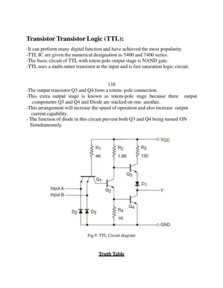
Transistor Biasing Circuits: A Comprehensive Overview
Biasing is crucial for the proper functioning of transistor circuits, ensuring they operate in the active region as amplifiers. This process involves setting DC voltages to establish the correct operating conditions for the transistor. By providing the necessary biasing, amplification of small input signals becomes feasible, enabling the transistor to function as an amplifier effectively. Understanding the importance of biasing, factors affecting the operating point, and the need for stabilization are key aspects for designing reliable transistor circuits.

Download Presentation

Please find below an Image/Link to download the presentation.
The content on the website is provided AS IS for your information and personal use only. It may not be sold, licensed, or shared on other websites without obtaining consent from the author. Download presentation by click this link. If you encounter any issues during the download, it is possible that the publisher has removed the file from their server.
E N D
Presentation Transcript
CHAPTER _ 11 TRANSISTOR BIASING CIRCUITS By MEENAKSHI MEHAN
BIASING Biasing is the process of providing DC voltage which helps in the functioning of the circuit. A transistor is based in order to make junction forward biased and collector base junction reverse biased, so that it maintains in active region, to work as an amplifier. the emitter base
TRANSISTOR BIASING The collector current and the maintenance of proper collector emitter voltage during the passage of signal is known as Transistor Biasing. which provides transistor biasing is called as Biasing Circuit proper flow of zero signal The circuit
NEED OF BIASING If a signal of very small voltage is given to the input of amplified. Because, for a BJT, to amplify a signal, two conditions have to be met. BJT, it cannot be The input voltage should exceed cut-in voltage for the transistor to be ON. The BJT should be in the active region, to be operated as an amplifier.
CONTD. If appropriate DC voltages and currents are given through sources, so that BJT operates in active region and superimpose the AC signals to be amplified, then this problem can be avoided. The given currents are so chosen that the transistor remains in active region for entire input AC cycle. Hence DC biasing is needed. BJT by external DC voltage and
The below figure shows a transistor amplifier that is provided with DC biasing on both input and output circuits. For a transistor to be operated as a faithful amplifier, the operating point should be stabilized.
Factors affecting the operating point The operating point shifts due to change in temperature. As temperature increases, the values of ICE, , VBEgets affected. ICBOgets doubled (for every 10orise) VBEdecreases by 2.5mv (for every 1orise) So the main problem which affects the operating point is temperature. Hence operating point should be made independent of the temperature so as to achieve stability. To achieve this, biasing circuits are introduced.
Stabilization The process of making the operating point independent of temperature changes or variations in transistor parameters is known as Stabilization. Once the stabilization is achieved, the values of ICand VCEbecome independent of temperature variations or replacement of transistor. A good biasing circuit helps in the stabilization of operating point
Need for Stabilization Stabilization of the operating point has to be achieved due to the following reasons. Temperature dependence of IC Individual variations Thermal runaway
Temperature Dependence of IC As the expression for collector current ICis IC= IB+ICEO IC = IB+( +1)ICBO The collector leakage current ICBO influenced by temperature variations. To come out of this, the biasing conditions are set so that zero signal collector current IC= 1 mA. Therefore, the operating point needs to be stabilized i.e. it is necessary to keep ICconstant. is greatly
Individual Variations As the value of and the value of VBEare not same for every transistor, whenever a transistor is replaced, the operating point tends to change. Hence it is necessary to stabilize the operating point.
Thermal Runaway As the expression for collector current IC is IC= IB+ICEO IC = IB+( +1)ICBO
Contd The flow of collector current and also the collector leakage current causes heat dissipation. If the operating point is not stabilized, there occurs a cumulative effect which increases this heat dissipation. The self-destruction of such an un-stabilized transistor is known as Thermal run away. In order to avoid destruction of transistor, it is necessary to stabilize the operating point, i.e., to keep ICconstant. thermal runaway and the
Stability Factor It is understood that ICshould be kept constant in spite of variations of ICBOor ICO. The extent to which a biasing circuit is successful in maintaining this is measured by Stability factor. It denoted by S. By definition, the rate of change of collector current ICwith respect to the collector leakage current ICOat constant and IBis called Stability factor S = dIc/dIco at constant and Ib
Contd Hence we can understand that any change in collector leakage current changes the collector current to a great extent. The stability factor should be as low as possible so that the collector current doesn t get affected. S=1 is the ideal value. The general expression of stability factor for a CE configuration can be obtained as under. IC = Ib+( +1)Ico
Contd Differentiating above expression with respect to IC, we get 1= dIB/dIC+( +1) dICO / dIC OR 1= dIB/dIC+( +1)/S [as dICO / dIC =1/S] S= +1/{1- (dIB/dIC)} Hence the stability factor S depends on , IBand IC.
Different biasing methods The commonly used methods of transistor biasing are Base Resistor method Collector to Base bias Biasing with Collector feedback resistor Voltage-divider bias All of these methods have the same basic principle of obtaining the required value of IBand ICfrom VCCin the zero signal conditions
Base Resistor Method In this method, a resistor RBof high resistance is connected in base, as the name implies. The required zero signal base current is provided by VCCwhich flows through RB. The base emitter junction is forward biased, as base is positive with respect to emitter. The required value of zero signal base current and hence the collector current (as IC= IB) can be made to flow by selecting the proper value of base resistor RB. Hence the value of RBis to be known. The figure below shows how a base resistor method of biasing circuit looks like.
Let ICbe the required zero signal collector current. Therefore IB = IC / Considering the closed circuit from VCC, base, emitter and ground, while applying the Kirchhoff s voltage law, we get, VCC=IBRB+VBE IBRB = VCC VBE Therefore RB =(VCC VBE )/IB
Since VBEis generally quite small as compared to VCC, the former can be neglected with little error. Then, RB = VCC / IB We know that VCCis a fixed known quantity and IBis chosen at some suitable value. As RBcan be found directly, this method is called as fixed bias method.
Stability factor S= +1/{1- (dIB/dIC)} In fixed-bias method of biasing, IBis independent of ICso that, dIB/dIC =0 Substituting the above value in the previous equation S= +1 Thus the stability factor in a fixed bias is ( +1) which means that ICchanges ( +1) times as much as any change in ICO.
Advantages The circuit is simple. Only one resistor REis required. Biasing conditions are set easily. No loading effect as no resistor is present at base- emitter junction
Disadvantages The stabilization is poor as heat development can t be stopped. The stability factor is very high. So, there are strong chances of thermal run away. Hence, this method is rarely employed
Collector to Base Bias The collector to base bias circuit is same as base bias circuit except that the base resistor RBis returned to collector, rather than to VCCsupply as shown in the figure below. This circuit helps in improving the stability considerably. If the value of ICincreases, the voltage across RLincreases and hence the VCEalso increases. This in turn reduces the base current IB. This action somewhat compensates the original increase. The required value of RBneeded to give the zero signal collector current ICcan be calculated as follows.
Circuit diagram Voltage drop across RLwill be RL(IC+IB)RL I C RL
Analysis From the figure, IC RL+I B RB+ VBE = VCC Or I B RB = VCC -IC RL VBE Therefore RB =[ VCC -IC RL VBE ]/IB RB=(VCC VBE ICRL) / IC According to KVL (IB+IC)RL+IBRB+VBE=VCC
Contd Therefore IB = [VCC VBE- IC RL ] / [RL + RB ] Since VBEis almost independent of collector current, we get dIB/dIC = - R L / RL + RB We know that S= +1/{1- (dIB/dIC)} therefore S= +1/{1- (- R L / RL + RB )}
Contd This value is smaller than (1+ ) which is obtained for fixed bias circuit. Thus there is an improvement in the stability. This circuit provides a negative feedback which reduces the gain of the amplifier. So the increased stability of the collector to base bias circuit is obtained at the cost of AC voltage gain.
Biasing with Collector Feedback resistor In this method, the base resistor RBhas its one end connected to base and the other to the collector as its name implies. In this circuit, the zero signal base current is determined by VCBbut not by VCC. It is clear that VCBforward biases the base-emitter junction and hence base current IBflows through RB. This causes the zero signal collector current to flow in the circuit. The below figure shows the biasing with collector feedback resistor circuit
Contd The required value of RBneeded to give the zero signal current ICcan be determined as follows VCC=ICRC+IBRB+VBE RB ={ VCC VBE ICRC } /IB here IB = IC / Stability factor is S < ( +1) this method provides better thermal stability than the fixed bias.
Advantages The circuit is simple as it needs only one resistor. This circuit provides some stabilization, for lesser changes. Disadvantages The circuit doesn t provide good stabilization. The circuit provides negative feedback
Voltage Divider Bias Method Among all the methods of providing biasing and stabilization, the voltage divider bias method is the most prominent one. Here, two resistors R1and R2are employed, which are connected to VCCand provide biasing. The resistor REemployed in the emitter provides stabilization. The name voltage divider comes from the voltage divider formed by R1and R2. The voltage drop across R2forward biases the base-emitter junction. This causes the base current and hence collector current flow in the zero signal conditions. The figure below shows the circuit of voltage divider bias method.
Suppose that the current flowing through resistance R1is I1. As base current IBis very small, therefore, it can be assumed with reasonable accuracy that current flowing through R2is also I1. Now let us try to derive the expressions for collector current and collector voltage. Collector Current, IC From the circuit, it is evident that
Contd I1 = Vcc / R1+ R2 Therefore, the voltage across resistance R2is V2 =( Vcc / R1+ R2 ) R2 Applying KVL VEV 2=VBE+VE VEV 2=VBE+IERE IE = {VEV 2 VBE } / IE As IE = Ic therefore IC = {VEV 2 VBE } / IE
Contd From the above expression, it is evident that ICdoesn t depend upon . VBEis very small that ICdoesn t get affected by VBEat all. Thus ICin this circuit is almost independent of transistor parameters and hence good stabilization is achieved
Collector-Emitter Voltage, VCE Applying Kirchhoff s voltage law to the collector side, VCC=ICRC+VCE+IERE On solving this expression we get VCE =VCC IC (RC RE ) Suppose there is a rise in temperature, then the collector current ICdecreases, which causes the voltage drop across REto increase. As the voltage drop across R2is V2, which is independent of IC, the value of VBEdecreases. The reduced value of IBtends to restore ICto the original value.
Stability Factor The equation for Stability factor of this circuit is obtained as S = ( +1)(R0+R3)/R0+RE+ RE ={( +1) 1+R0/RE }/{ +1+R0/RE } If the ratio R0/REis very small, then R0/RE can be neglected as compared to 1 and the stability factor becomes equal to 1 This is the smallest possible value of S and leads to the maximum possible thermal stability