Understanding Sequential Logic in NUS CS2100 Lecture #19
Explore the concepts of sequential logic in Lecture #19 by Aaron Tan at NUS, covering memory elements, latches, flip-flops, asynchronous inputs, synchronous sequential circuits, and different types of sequential circuits. Delve into the distinction between combinatorial and sequential circuits, memory units, read/write operations, and memory arrays. Learn about bistable logic devices, latches, flip-flops, memory elements with clocks, and various triggering/activation methods in the realm of sequential logic design.

Download Presentation

Please find below an Image/Link to download the presentation.
The content on the website is provided AS IS for your information and personal use only. It may not be sold, licensed, or shared on other websites without obtaining consent from the author. Download presentation by click this link. If you encounter any issues during the download, it is possible that the publisher has removed the file from their server.
E N D
Presentation Transcript
http://www.comp.nus.edu.sg/~cs2100/ Lecture #19 Sequential Logic https://app.sli.do/event/aanrHmK6Geu3scZbeLh6wx
Aaron Tan, NUS Lecture #19: Sequential Logic 2 Lecture #19: Sequential Logic (1/2) 1. Introduction 2. Memory Elements 3. Latches 3.1 S-R Latch 3.2 D Latch 4. Flip-flops 4.1 S-R Flip-flop 4.2 D Flip-flop 4.3 J-K Flip-flop 4.4 T Flip-flop
Aaron Tan, NUS Lecture #19: Sequential Logic 3 Lecture #19: Sequential Logic (2/2) 5. Asynchronous Inputs 6. Synchronous Sequential Circuit 6.1 Flip-flop Characteristic Tables 6.2 Analysis 6.3 Flip-flop Excitation Tables 6.4 Design 7. Memory 7.1 Memory Unit 7.2 Read/Write Operations 7.3 Memory Cell 7.4 Memory Arrays
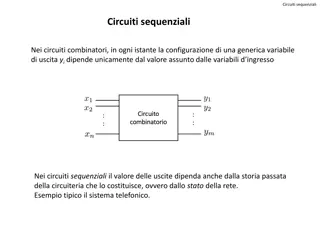
Aaron Tan, NUS Lecture #19: Sequential Logic 4 1. Introduction (1/2) Two classes of logic circuits Combinational Sequential Sequential Circuit Each output depends on both present inputs and state. Combinational Circuit Each output depends entirely on the immediate (present) inputs. Combinational Logic Combinational Logic inputs : : : : outputs inputs : : : : outputs Memory
Aaron Tan, NUS Lecture #19: Sequential Logic 5 1. Introduction (2/2) Two types of sequential circuits: Synchronous: outputs change only at specific time Asynchronous: outputs change at any time Multivibrator: a class of sequential circuits Bistable (2 stable states) Monostable or one-shot (1 stable state) Astable (no stable state) Bistable logic devices Latches and flip-flops. They differ in the methods used for changing their state.
Aaron Tan, NUS Lecture #19: Sequential Logic 6 2. Memory Elements (1/3) Memory element: a device which can remember value indefinitely, or change value on command from its inputs. Q Memory element command stored value Characteristic table: Command (at time t) Q(t) Q(t+1) Q(t) or Q: current state Set X 1 Q(t+1) or Q+: next state Reset X 0 Memorise / No Change 0 1 0 1
Aaron Tan, NUS Lecture #19: Sequential Logic 7 2. Memory Elements (2/3) Memory element with clock. Q Memory element command stored value clock Clock is usually a square wave. Positive pulses Positive edges Negative edges
Aaron Tan, NUS Lecture #19: Sequential Logic 8 2. Memory Elements (3/3) Two types of triggering/activation Pulse-triggered Edge-triggered Positive pulses Pulse-triggered Latches ON = 1, OFF = 0 Positive edges Negative edges Edge-triggered Flip-flops Positive edge-triggered (ON = from 0 to 1; OFF = other time) Negative edge-triggered (ON = from 1 to 0; OFF = other time)
Aaron Tan, NUS Lecture #19: Sequential Logic 9 3.1 S-R Latch (1/3) Two inputs: S and R. Two complementary outputs: Q and Q'. When Q = HIGH, we say latch is in SET state. When Q = LOW, we say latch is in RESET state. For active-high input S-R latch (also known as NOR gate latch) R = HIGH and S = LOW Q becomes LOW (RESET state) S = HIGH and R = LOW Q becomes HIGH (SET state) Both R and S are LOW No change in output Q Both R and S are HIGH Outputs Q and Q' are both LOW (invalid!) Drawback: invalid condition exists and must be avoided.
Aaron Tan, NUS Lecture #19: Sequential Logic 10 3.1 S-R Latch (2/3) Active-high input S-R latch: S 1 0 0 0 1 R 0 0 1 0 1 Q 1 1 0 0 0 Q' 0 0 1 1 0 R 1 0 1 0 0 1 1 0 0 0 Q initial (afer S=1, R=0) Q' 0 0 1 1 0 (after S=0, R=1) invalid! 1 0 0 0 1 S Block diagram: S Q R Q'
Aaron Tan, NUS Lecture #19: Sequential Logic 11 3.1 S-R Latch (3/3) S Q Characteristic table for active-high input S-R latch: R Q' S R Q Q' No change. Latch remained in present state. Latch SET. Latch RESET. Invalid condition. 0 0 NC NC 1 0 1 0 1 1 1 0 0 0 1 0 S R Q(t+1) Q(t) 0 1 0 0 1 1 0 1 0 1 No change Reset Set Q(t+1) = ? S + R' Q S R = 0 indeterminate
Aaron Tan, NUS Lecture #19: Sequential Logic 12 3.1 Active-Low S-R Latch (You may skip this slide.) What we have seen is active-high input S-R latch. There are active-low input S-R latches, where NAND gates are used instead. See diagram on the left below. S Q S Q Q' Q' R R In this case, when R=0 and S=1, the latch is reset (i.e. Q becomes 0) when R=1 and S=0, the latch is set (i.e. Q becomes 1) when S=R=1, it is a no-change command. when S=R=0, it is an invalid command. Sometimes, we use the alternative gate diagram for the NAND gate. See diagram on the right above. (This appears in more complex latches/flip-flops in the later slides.) (Sometimes, the inputs are labelled as S' and R'.)
Aaron Tan, NUS Lecture #19: Sequential Logic 13 3.1 Gated S-R Latch S-R latch + enable input (EN) and 2 NAND gates a gated S-R latch. S Q S Q EN EN Q' Q' R R Outputs change (if necessary) only when EN is high.
Aaron Tan, NUS Lecture #19: Sequential Logic 14 3.2 Gated D Latch (1/2) Make input R equal to S' gated D latch. D latch eliminates the undesirable condition of invalid state in the S-R latch. D Q D Q EN EN Q' Q'
Aaron Tan, NUS Lecture #19: Sequential Logic 15 3.2 Gated D Latch (2/2) When EN is high, D = HIGH latch is SET D = LOW latch is RESET Hence when EN is high, Q follows the D (data) input. Characteristic table: EN D Q(t+1) 1 1 0 0 1 X 0 1 Reset Set No change Q(t) When EN=1, Q(t+1) = ? D
Aaron Tan, NUS Lecture #19: Sequential Logic 16 4. Flip-flops (1/2) Flip-flops are synchronous bistable devices. Output changes state at a specified point on a triggering input called the clock. Change state either at the positive (rising) edge, or at the negative (falling) edge of the clock signal. Clock signal Positive edges Negative edges
Aaron Tan, NUS Lecture #19: Sequential Logic 17 4. Flip-flops (2/2) S-R flip-flop, D flip-flop, and J-K flip-flop. Note the > symbol at the clock input. S D J Q Q Q C C C Q' Q' Q' R K Positive edge-triggered flip-flops S D J Q Q Q C C C Q' Q' Q' R K Negative edge-triggered flip-flops
Aaron Tan, NUS Lecture #19: Sequential Logic 18 4.1 S-R Flip-flop S-R flip-flop: On the triggering edge of the clock pulse, R = HIGH and S = LOW Q becomes LOW (RESET state) S = HIGH and R = LOW Q becomes HIGH (SET state) Both R and S are LOW No change in output Q Both R and S are HIGH Invalid! Characteristic table of positive edge-triggered S-R flip- flop: S R CLK Q(t+1) Comments Q(t) 0 1 ? 0 0 1 1 0 1 0 1 X No change Reset Set Invalid S Q C Q' R X = irrelevant ( don t care ) = clock transition LOW to HIGH
Aaron Tan, NUS Lecture #19: Sequential Logic 19 4.2 D Flip-flop (1/2) D flip-flop: Single input D (data). On the triggering edge of the clock pulse, D = HIGH Q becomes HIGH (SET state) D = LOW Q becomes LOW (RESET state) Hence, Q follows D at the clock edge. Convert S-R flip-flop into a D flip-flop: add an inverter. D S Q D CLK Q(t+1) Comments C CLK 1 0 1 0 Set Reset Q' R = clock transition LOW to HIGH A positive edge-triggered D flip- flop formed with an S-R flip-flop.
Aaron Tan, NUS Lecture #19: Sequential Logic 20 4.2 D Flip-flop (2/2) Application: Parallel data transfer. To transfer logic-circuit outputs X, Y, Z to flip-flops Q1, Q2 and Q3 for storage. D Q Q1 = X* CLK Q' X Combinational logic circuit Y D Q Q2 = Y* Z CLK Q' D Q Q3 = Z* Transfer CLK Q' * After occurrence of negative-going transition
Aaron Tan, NUS Lecture #19: Sequential Logic 21 4.3 J-K Flip-flop (1/2) J-K flip-flop: Q and Q' are fed back to the pulse-steering NAND gates. No invalid state. Include a toggle state J = HIGH and K = LOW Q becomes HIGH (SET state) K = HIGH and J = LOW Q becomes LOW (RESET state) Both J and K are LOW No change in output Q Both J and K are HIGH Toggle
Aaron Tan, NUS Lecture #19: Sequential Logic 22 4.3 J-K Flip-flop (2/2) J-K flip-flop circuit: J Q Pulse transition detector CLK Q' K Characteristic table: Q J K Q(t+1) 0 0 0 0 1 1 1 1 0 0 1 1 0 0 1 1 0 1 0 1 0 1 0 1 0 0 1 1 1 0 1 0 J K CLK Q(t+1) Comments Q(t) 0 1 Q(t)' 0 0 1 1 0 1 0 1 No change Reset Set Toggle Q(t+1) = ? J Q' + K' Q
Aaron Tan, NUS Lecture #19: Sequential Logic 23 4.4 T Flip-flop T flip-flop: Single input version of the J-K flip-flop, formed by tying both inputs together. T T Q J Q Pulse transition detector C CLK CLK Q' Q' K Characteristic table: Q T Q(t+1) T CLK Q(t+1) Comments 0 0 1 1 0 1 0 1 0 1 1 0 Q(t) Q(t)' 0 1 No change Toggle Q(t+1) = ? T Q' + T' Q
Aaron Tan, NUS Lecture #19: Sequential Logic 24 5. Asynchronous Inputs (1/2) S-R, D and J-K inputs are synchronous inputs, as data on these inputs are transferred to the flip-flop s output only on the triggered edge of the clock pulse. Asynchronous inputs affect the state of the flip-flop independent of the clock; example: preset (PRE) and clear (CLR) [or direct set (SD) and direct reset (RD)]. When PRE=HIGH, Q is immediately set to HIGH. When CLR=HIGH, Q is immediately cleared to LOW. Flip-flop in normal operation mode when both PRE and CLR are LOW.
Aaron Tan, NUS Lecture #19: Sequential Logic 25 5. Asynchronous Inputs (2/2) A J-K flip-flop with active-low PRESET and CLEAR asynchronous inputs. PRE PRE J Q J Q Pulse transition detector C CLK Q' K Q' K CLR CLR CLK PRE CLR Q J = K = HIGH Preset Toggle Clear
Aaron Tan, NUS Lecture #19: Sequential Logic 26 End of File