Understanding Combinational Circuits in Digital Systems

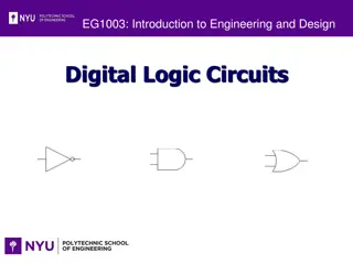
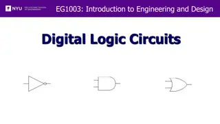
Combinational circuits in digital systems consist of logic gates interconnected to process input signals and produce output based solely on the current input, without any memory. They are implemented using basic logic gates like NAND, NOR, or NOT gates, which can be combined to create complex switching circuits. The half-adder, a fundamental arithmetic circuit for binary addition, is discussed, along with its limitations and the development of full adders to overcome these limitations. The design, implementation, and logic expressions for both half-adders and full adders are elaborated.

Download Presentation

Please find below an Image/Link to download the presentation.
The content on the website is provided AS IS for your information and personal use only. It may not be sold, licensed, or shared on other websites without obtaining consent from the author. Download presentation by click this link. If you encounter any issues during the download, it is possible that the publisher has removed the file from their server.
E N D
Presentation Transcript
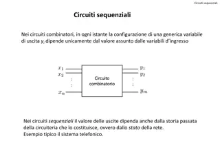
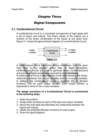
Computer System Architecture COMP201TH Lecture-7 Combinational Circuits Combinational Circuits: o A combinational circuit is a connected arrangement of logic gates with a set of inputs and outputs. o The behaviour of a combinational circuit is memoryless i.e. the output depends solely on its most recent input and is independent of the circuit s past history. o In general term, a combinational circuit consists of n binary inputs and m binary outputs. o Combinational Logic circuits are made up from basic logic NAND, NOR or NOT gates that are combined or connected together to produce more complicated switching circuits. o Any combinational circuit can be implemented with only NAND and NOR gates as these are classified as universal gates. o As with logic gates, a combinational circuit can be defined in three ways: Truth Table: For each of the 2npossible combinations of input signals, the binary value of each of the m output signal is listed. Graphical Symbols: The interconnected layout of gates is depicted. Boolean Equations: Each output signal is expressed as a Boolean function of its input signals. Pag e 57
Representation of Combinational Logic Circuits Common combinational circuits made up from individual logic gates that carry out a desired application include Multiplexer, De-multiplexers, Encoders, Decoders, Full and Half Adders etc. Classification of Combinational Logic: Pag e 58
Half Adder: o The most basic digital arithmetic circuit is the addition of two binary digits. o A combinational circuit that performs the arithmetic addition of two bits is called a half-adder. Half-adder truth table and implementation S = A`B+AB` = A B C = AB To implement half adder using NAND gates; we require 5 NAND gates. o 0+1 = 1 +0 =1 S=1, C= 0 1+1 = 10 S=0, C=1 Pag e 59 1+1+1 = 11 S=1, C=1
Limitations of Half Adder: o The reason it s called half adder is that there is no scope to add the carry bit from previous bit. This is a major limitation of half adders when used as binary adders especially in real time scenarios which involves addition of multiple bits. o To overcome this limitation, full adders are developed. Full Adder: o A full-adder is a combinational circuit that performs the arithmetic sum of three input bits. Block Diagram of Full Adder Logic Diagram of Full Adder o The full adder can be thought of as two half adders connected together, with the first half adder passing its carry to the second half adder. Pag e 60 o
o Truth Table for Full Adder is: o The Boolean Expression for a full adder is: Sum = (A B) Cin C-Out = A.B + Cin(A B) = AB+ACin+BCin AB+ACin+BCin = AB + ACin+BCin(A+A`) = ABCin+AB+ACin+A`BCin = AB(1+Cin)+ACin+A`BCin = AB+ACin+A`BCin =AB+ACin(B+B`)+A`BCin =ABCin+AB+AB`Cin+A`BCin =AB(1+Cin)+AB`Cin+A`BCin =AB+AB`Cin+A`BCin Pag e 61 =AB+Cin(AB`+A`B) = AB+Cin(A B)