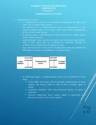
Analysis of Clocked Sequential Circuits and Parity Checkers
This chapter delves into the analysis of clocked sequential circuits, focusing on topics such as sequential parity checkers, signal tracing, state tables and graphs, and models for sequential circuits. It covers concepts like Mealy and Moore machines, state equations, state graphs, timing charts, and more. The content includes block diagrams, sample waveforms, state tables, next-state tables, and detailed explanations on how to analyze sequential circuits using various methods.

Download Presentation

Please find below an Image/Link to download the presentation.
The content on the website is provided AS IS for your information and personal use only. It may not be sold, licensed, or shared on other websites without obtaining consent from the author. Download presentation by click this link. If you encounter any issues during the download, it is possible that the publisher has removed the file from their server.
E N D
Presentation Transcript
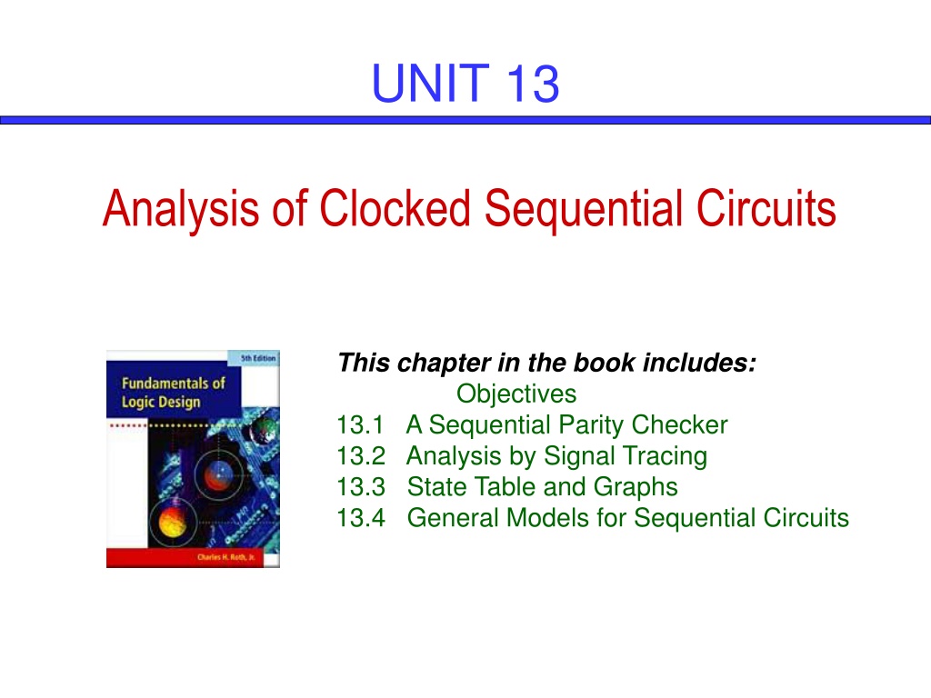
UNIT 13 Analysis of Clocked Sequential Circuits This chapter in the book includes: Objectives 13.1 A Sequential Parity Checker 13.2 Analysis by Signal Tracing 13.3 State Table and Graphs 13.4 General Models for Sequential Circuits
Objectives 1. Analysis of a sequential circuit by signal tracing 2. For a given a sequential circuit Write the next-state equations for the flip-flops Derive the state graph or state table. Using the state graph, determine The state sequence Output sequence 3. Mealy machine and Moore machine 4. Given a state table, Construct the corresponding state graph 5. Given a sequential circuit or a state table and an input sequence, Draw a timing chart for the circuit. Determine the output sequence from the timing chart 6. Draw a general model for a clocked Mealy or Moore sequential circuit
13.1 A Sequential Parity Checker 8-bit Words with Odd Parity
13.1 A Sequential Parity Checker Block Diagram for 8-Bit Odd Parity Checker Z=1 if input parity is odd
13.1 A Sequential Parity Checker Sample Waveforms for Parity Checker
13.1 A Sequential Parity Checker State Graph for Parity Checker Even number of 1 received Odd number of 1 received
13.1 A Sequential Parity Checker State Table for Parity Checker Present Next State Present State X = 0 X = 1 Output 0 S0 S0 S1 1 S1 S1 S0
13.1 A Sequential Parity Checker Next-State Table for Parity Checker Using T F/F Q = 0 for S0, Q = 1 for S1 Present State S0 Next State X = 0 X = 1 S0 S1 Present Output 0 Q Q+ T Z X = 0 X = 1 0 1 X = 0 X = 1 0 1 0 0 1 1 0 0 1 1 1 S1 S1 S0 Parity Checker
13.2 Analysis by Signal Tracing and Timing Charts Output tracing 1. Assume an initial state of F/F (All flip-flops reset to 0) 2. For the first input in the give sequence, determine the output and F/F inputs 3. Determine the new sets of F/F states after the next clock edge 4. Determine the output that corresponds to the new states 5. Repeat 2,3,4 for each in the given sequence
13.2 Analysis by Signal Tracing and Timing Charts Moore Machine The output is a function of the present state only The state graph has the output associated with the state
13.2 Analysis by Signal Tracing and Timing Charts Mealy Machine The output is a function of the present state and the input The state graph has the output associated with the arrow
13.2 Analysis by Signal Tracing and Timing Charts Moore Sequential Circuit to be Analyzed Input sequence X=01101 DA = X xor B DB = A + B
13.2 Analysis by Signal Tracing and Timing Charts Timing Chart for Figure 13-5 DA = X xor B DB = A + B X = 0 1 1 0 1 A = 0 1 0 1 0 1 B = 0 0 1 1 1 1 Z = (0) 1 1 0 1 0
13.2 Analysis by Signal Tracing and Timing Charts Mealy Sequential Circuit to be Analyzed Input sequence X=10101
13.2 Analysis by Signal Tracing and Timing Charts Mealy Sequential Circuit to be Analyzed X = 1 0 1 0 1 A = 0 0 0 1 1 0 B = 0 1 1 1 1 0 Z = 1(0) 1 0(1) 0 1 (False outputs are indicated in parentheses) Timing Chart JA = X B KA = X JB = X KB = X A
13.2 Analysis by Signal Tracing and Timing Charts False outputs: Glitches or Spikes
13.3 State Table and Graphs Systematic Approach to Analyze Sequential Circuits 1. Determine the flip-flop input equations and the output equations from the circuit. 2. Derive the next-state equation for each flip-flop from its input equations, using one of the following relations: D flip-flop Q+= D D-CE flip-flop Q+= D CE + Q CE T-flip-flop Q+= T XOR Q S-R flip-flop Q+= S + R Q J-K flip-flop Q+= JQ + K Q 3. Plot a next-state equations for the flip-flop. 4. Combine these maps to form the state table. Such a state table, which gives the next state of the flip-flops as a function of their present state and the circuit inputs, is frequently referred to as a transition table. (13-1) (13-2) (13-3) (13-4) (13-5)
13.3 State Table and Graphs Example: To derive the State Table (Moore Machine) 1. Flip-flop Input equations and Output equations B= + = A= ' D X B D X A Z A B
13.3 State Table and Graphs Example: To derive the State Table 1. Flip-flop Input equations and Output equations D X B ' D B= + = A= X A Z A B 2. The next-state A + + = = + ' X B B X A
13.3 State Table and Graphs Example: To derive the State Table 2. The next-state A + + = = + ' X B B X A 3. Karnaugh Maps + = ' XB + A X B + = ' ' X B = + ( X ' AB + ' )( A ) ' XAB X B XB + A A = + + ' ' ' ' ' ' X B XA B + = B X A + = + + + + ( ' )( ) ' ( XA )( XAB ' ) ' XAB + X A A B B A + X X + B B = + + + + + ' ' ' ' ' ' ' ' XAB XAB XA B B X AB X AB = + + + + ' ' ' ' ' ' ' XAB XAB XA B XA B X AB X AB
13.3 State Table and Graphs 4. To Derive a Transition Table A+B+ Present State S0 S1 S2 S3 Next State X = 0 X = 1 S3 S0 S2 S1 S2 Present Output (Z) 0 1 0 1 AB 00 01 11 10 X = 0 X = 1 10 01 00 11 01 11 11 01 Z 0 1 0 1 S1 S2 S1
13.3 State Table and Graphs State Graph for Moore Machine state Present State Next State X = 0 X = 1 Present Output (Z) input S0 S1 S2 S3 S3 S0 S2 S1 S2 S1 0 1 0 1 S2 S1 output
13.3 State Table and Graphs Example: To derive the State Table (Mealy Machine) The next-state and output equations are + = = + + = = + + ' ' ' X A ' A J A K A A XBA A + + ' ( = + + ' ' )' ' X B ' A B ' B Z J B K B X A B ' ' XB XA AX B XB B B = + ' XB
11.6 J-K Flip-Flop J-K Flip-Flop (Rising Edge Trigger Type) Q+ 0 1 0 0 1 1 1 0 J K Q 0 0 0 0 0 1 0 1 0 0 1 1 1 0 0 1 0 1 1 1 0 1 1 1 Q=0 Q=1 JK=00 0 1 JK=01 0 0 JK=11 1 0 JK=10 1 1 Q + = + Q J Q K Next state table and characteristic equation
13.3 State Table and Graphs The next-state and output maps = + = + = + ' ' + = = + + ' ' ' X A ' A J A K A A XBA A + + ' ( = + + ' ' )' ' X B ' A B ' B Z J B K B X A B XB XA AX B XB B B ' XB
13.3 State Table and Graphs Transition Table A+B+ Z Present State S0 S1 S2 S3 Next State X = 0 1 S0 S1 S2 S0 S3 Present Output X = 0 1 0 1 1 0 0 1 0 1 AB 00 01 11 10 X = 0 1 00 01 01 11 11 00 10 01 X = 0 1 0 1 1 0 0 1 0 1 S1 S2 S1
13.3 State Table and Graphs State Graph for Mealy Machine Present State Next State X = 0 1 Present Output X = 0 1 input S0 S1 S2 S3 S0 S1 S2 S0 S3 S1 S2 0 1 1 0 0 1 0 1 output S1 state
13.3 State Table and Graphs Serial Adder xi 0 0 0 0 0 1 0 1 0 0 1 1 1 0 0 1 0 1 1 1 0 1 1 1 yi ci ci+1 0 0 0 1 0 1 1 0 0 1 1 0 1 0 1 1 si (b) Truth table
13.3 State Table and Graphs Timing Diagram for Serial Adder
13.3 State Table and Graphs State Graph for Serial Adder
13.3 State Table and Graphs Construction and Interpretation of Timing Chart 1. When constructing timing charts, note that a state change can only occur after the rising (or falling) edge of the clock, depending on the type of flip-flop used. 2. The input will normally be stable immediately before and after the active clock edge. 3. For a Moore circuit, the output can change when the input changes as well as when the state changes. A false may occur between the state changes and the time the input is changed to its new value. ( In other words, if the state has changed to its next value, but the old input is still present, the output may be temporally incorrect.) 4. False outputs are difficult to determine from the state graph, so use either signal tracing through the circuit or use the state table when constructing timing charts for Mealy circuit. 5. When using a Mealy state table for constructing timing charts, the procedure is as follows: a) for the first input, read the present output and plot it. b) Read the next state and plot it (following the active edge of the clock pulse). c) Go to the row in the table which corresponds to the next state and read the output under the old input column and plot it d) Change to the next input and repeat step (a) (b) and ( c). 6. For Mealy circuits, the best time to read the output is just before the active edge of the clock, because the output should always be correct at that time.0
13.4 General Models for Sequential Circuit General Model for Mealy Circuit Using Clocked D Flip-Flops
13.4 General Models for Sequential Circuit The combinational subcircuit realizes the n output functions and the k next- state function, which serve as inputs to the D flip-flop. = = . . . = ( , .... .... , , ,.... ,.... ) Z Z f X X f X X 2 ( X X Q Q Q Q 1 , Q Q 1 1 1 2 1 2 m k , , ) 2 1 2 2 n output functions m k ( X X 1 , .... , Q Q 1 , ,.... ) Z f X Q 2 2 2 n m k + = = . . . = = g X X 1 ( ( , .... , Q Q 1 , , ,.... ) Q D X Q 1 + 1 1 2 2 m k , .... Q Q 1 , ,.... ) Q D g X X 2 X Q 2 2 1 2 2 m k k next-state functions += = ( X X , 1 .... , Q Q , 1 ,.... ) Q D g X Q 2 2 k k k m k
13.4 General Models for Sequential Circuit Minimum Clock Period for a Sequential Circuit (min) = + + t t t t clk p c su (min) = + + t t t t clk x c su
13.4 General Models for Sequential Circuit General Model for Moore Circuit Using Clocked D Flip-Flops
13.4 General Models for Sequential Circuit State Table with Multiple inputs and Outputs Present State Present Output(z) Next state = = 01 10 11 00 00 X X 1 X X 1 11 01 10 2 2 S0 S3 S0 S3 S1 2 S S1 S0 2 S 0 2 2 3 3 0 2 3 1 0 0 1 1 2 3 1 S1 S1 S0 2 S S3 2 S S3 S1 S1S0 2 S += ( , ) S S X = ( , ) Z S X = = = = ( ( , ) , ) 3 3 ( ( , ) , ) 1 1 S S S 1 S S S 2 2 1 0 2 2 0