Understanding Diode Circuits: Half-Wave Rectifiers and Full-Wave Rectifiers
Diode circuits play a crucial role in converting AC signals to DC signals. This article covers the basics of diodes, half-wave rectifiers, and full-wave rectifiers. It explains the functioning of unfiltered and filtered rectifier circuits, highlighting the differences in ripple effects and voltage regulation. By exploring these concepts, readers can gain a comprehensive understanding of rectifier circuits and their applications.
Download Presentation

Please find below an Image/Link to download the presentation.
The content on the website is provided AS IS for your information and personal use only. It may not be sold, licensed, or shared on other websites without obtaining consent from the author. Download presentation by click this link. If you encounter any issues during the download, it is possible that the publisher has removed the file from their server.
E N D
Presentation Transcript
ENEE 205 Diode circuits Part 1: Half-wave rectifiers
The basic diode ID The symbol for the diode is on the left (a). The diode can conduct current with little voltage drop when it flows from the P side to the N side (b). Current can not flow in the opposite direction due to the formation of the depletion region (c). The ideal model for diode performance is indicated in the figure on the right (a). The actual I-V dependence is exponential (b), but an intermediate model (c) has a cutin voltage ?? and an internal resistance marked by a finite slope. (a) (a) + VD - VD e- e+ e- e- p n ID I (b) e- (b) depletion region VD e+ e- p n ID e- IO (c) (c) VD V Figure 12.1 The pn diode, The PN diode Figure 12.2. Diode circuit models Diode models
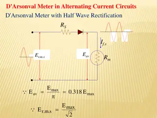
UNFILTERED HALF-WAVE RECTIFIER CIRCUIT (a) The half-wave rectifier circuit is shown on the left (a). A single diode is placed between the sinusoidal source and the resistive load. The voltage source signal is shown on the right (a). For each half period that the source voltage is positive, current will flow clockwise in the circuit and the diode model is shown on the left (b) as a voltage drop ??. Thus the current flows through the resistor during those half- periods as shown on the right (b). For each half period that the source voltage is negative, current would try to pass counterclockwise, but the diode would turn off and no current would pass ((c) on the left). Thus, the total current through the resistor is shown in (b) on the right. Since the average source voltage is zero, but the resistor voltage is never negative, we have (partially) rectified the voltage source. (b) (c)
FILTERED HALF-WAVE RECTIFIER CIRCUIT One application of these rectifier circuits is to convert an AC signal into a DC signal. As one can see from the last slide, a half-wave unfiltered rectifier is grossly inadequate for that purpose. On the following slides, we will progress through a sequence of circuits that bring us closer to building a DC source. We filter a circuit by placing a capacitor in parallel with the output load as shown in the figure on the left. When the diode is on (for the most part when the source voltage is positive), the capacitor charges in parallel with the resistor, but when the diode is off, we get a first-order transient problem excited by initial conditions and the voltage exponentially decays through the resistor. The net output voltage is approximated on the right. There is an initial ramp up from zero when the source is turned on, but later the voltage never returns to zero. We define the voltage ripple to be the percent variation from max voltage to min voltage. For the unfiltered case the ripple was 100%. For this filtered case, the ripple is much reduced and we are getting closer to a dc signal.
ENEE 205 Diode circuits Part 2: Full wave rectifiers
UNFILTERED FULL-WAVE RECTIFIER CIRCUIT To reduce the ripple on the half-wave rectifier circuit, one needs only to increase the filter capacitance, but that can quickly become bulky and expensive. A full-wave rectifier is made by placing a 4-diode bridge between the source and the resistive load as shown on the left (a). The full wave rectifier has important advantages over the half-wave circuit, but two potential disadvantages. First, the source and the load can no longer share the same ground. Second, the diode voltage drop is now always 2??. The latter restriction is usually important if the source voltage is only a few volts. For each half-period when the voltage source is positive, diodes D1 and D4 are off and current flows through the output resistor RL from top to bottom ((b) in both figures). When the voltage source is negative, diodes D2 and D3 are off and current flows through the output resistor RL from top to bottom ((c) in both figures). The net result is that we are using 100% if the input voltage and get full rectification (figure (d) on the right, albeit with 100% ripple.
FILTERED FULL-WAVE RECTIFIER CIRCUIT Again, we filter the circuit by placing a capacitor in parallel with the output load as shown in the figure on the left. For the unfiltered circuit, there are always two diodes that are on. Each pair (for example when D2 and D3 are on) allows one half of the sinusoidal signal to pass through. First, the voltage rises and the capacitor charges. But when the voltage drops, the capacitor is discharging, and it can only discharge through the resistor since current can not go backwards through the diodes. If RC is large enough, the capacitor can t discharge fast enough and all the diodes cut off, and we again are left with a first-order transient problem excited by initial conditions, and the voltage exponentially decays through the resistor. The net output voltage is approximated on the right. There is an initial ramp up from zero when the source is turned on, but later the voltage never returns to zero. We expect the voltage ripple to be much less than that of the half-wave rectifier, because the period of the full-wave output signal is half that of the half- wave rectifier (assuming the same values for the capacitor and the resistor.) On the next page we simulate three filter cases with the same output load and same capacitance to show the relative performance of the circuits.
Pspice simulation of rectifier circuits D2 1N4148 V1 VOFF = 0 V VAMPL = 10 FREQ = 60 AC = C1 470u R2 50 Four volt ripple GND_0 Half-wave filtered 0 D2 100% ripple 1N4148 D4 1N4148 D5 1N4148 V1 VOFF = 0 V VAMPL = 10 D3 FREQ = 60 AC = R2 50 1N4148 GND_0 Full-wave unfiltered 0 D2 1N4148 D4 1N4148 D5 1N4148 V1 VOFF = 0 V VAMPL = 10 D3 C1 470u FREQ = 60 AC = R2 50 1.7 volt ripple 1N4148 GND_0 Full-wave filtered 0
ENEE 205 Diode circuits Part 3: Zener diodes
I The Zener diode For most diodes, if you exceed some maximum reverse voltage, they are destroyed by what is called reverse breakdown . Some diodes can actually be fabricated to allow a reverse breakdown without damaging the diode (below a certain current level). When this happens, it is called zener breakdown and the diode is called a zener diode. The symbol for a zener diode and the V-I terminal relationship are given on the right. Notice that the slope of the V-I curve at the zener breakdown voltage is very sharp. This means that a zener diode can be used to maintain a nearly constant voltage over a wide range of currents. For this reason, zener diodes are often used in voltage regulation circuits for constant dc power supplies. Care must be taken in the designs so that the Zener is always at least a little on (to regulate) but so that it doesn t draw too much current to overheat and destroy the Zener. This means selecting an appropriate resistance between the filter capacitor and the Zener. If the resistance is too low, the Zener can overheat. If the resistance is too high, the Zener can cut off. zener diode -VZ V Figure 12.3 The Zener Diode. Zener Diode model
ZENER DIODES AND LINEAR RECTIFIERS D2 1N4148 D4 1N4148 D5 1N4148 V1 Full-wave filtered circuit VOFF = 0 V VAMPL = 10 D3 C1 470u FREQ = 60 AC = R2 50 1N4148 GND_0 Modifications to reduce ripple with Zener 0 D2 R1 2 1N4148 D4 1N4148 D5 1N4148 V1 VOFF = 0 VAMPL = 10 D3 C1 470u D1 D1N750 V FREQ = 60 AC = R2 50 1N4148 GND_0 0 ????? ?????? 2?????? ?????? < ?1< ?2(0.9(????? 2??????)/?????? 1) 7.8 < ?1< 32
Zener ripple for different filter resistances Output voltage R=2 OHMS Zener current R=10 OHMS
R=20 OHMS R=32 OHMS
ENEE 205 Diode circuits Part 4: Switching circuit
SWITCHING SUPPLIES The old-fashioned way to store energy in a circuit was to charge a capacitor through a resistor up to the needed voltage. This technique is inefficient in that at least 50% of the energy is lost to heat. The reason for this is that the most inefficient part of the process occurs at the beginning, when the capacitor has zero volts on it and the power dissipated in the resistor is greatest. As the capacitor voltage increases, the resistor power loss decreases, but the efficiency only reaches 50% when the capacitor reaches the charging voltage.
SWITCHING SUPPLIES A better way to store energy is to charge an inductor through a resistor, because the most efficient part of the process is at the beginning. However (1) the process becomes less and less efficient as time goes on, and (2) we still need to get the energy into a capacitor. (Unless your inductor is a super conductor, you can t store the energy there indefinitely.) The switching supply is a circuit that takes advantage of this idea to charge capacitors with 80-90% efficiency. Consider the simplified circuit shown above. The switch will open and close periodically, hence the double arrow. In fact, a MOSFET often functions as both the switch and the charging resistance.
SWITCHING SUPPLIES When the circuit is first assembled, the MOSFET/switch is unimportant and the inductor resonantly charges the capacitor to almost twice the battery voltage in a time ? = ? ??. At that point, if the switch is open, current is blocked by the diode. When the switch closes, The inductor starts to draw current with a time constant L/R, where R is the series combination of the inductor resistance and the switch resistance. When the switch opens, the inductor loses its path and must find another (recall inductor current must be continuous). The inductor voltage thus jumps up, the diode turns on, and the current passes into the capacitor to increase its voltage. The cycle repeats and the capacitor voltage can increase indefinitely until limited by nonideal circuit properties (e.g. resistance, diode reverse leakage current).
L1 D2 V1 20mH 1N4148 I 10Vdc Pspice simulations C1 470u R2 1Meg 10.00V 9.632V Q1 V1 = 0 V2 = 15 10.00V GND_0 V2 TD = 0 TR = 5u 3SK136 TF = 5u PW = 800u PER = 1.3m 0V 0 Inductor charging current 0V Initial resonant charge of capacitor Incremental energy pulses Capacitor Voltage (note vastly different time scale) Charges to 12 times battery voltage and counting!


