Digital Logic Design Lecture 6: Universal Gates and Gate Realizations
In Lecture 6 of Digital Logic Design, we delve into Universal Gates and their significance in implementing all Boolean functions. The discussion covers NAND and NOR gates as universal gates, their properties, and realizations. Understanding these concepts is crucial for designing efficient digital logic circuits.

Download Presentation

Please find below an Image/Link to download the presentation.
The content on the website is provided AS IS for your information and personal use only. It may not be sold, licensed, or shared on other websites without obtaining consent from the author. Download presentation by click this link. If you encounter any issues during the download, it is possible that the publisher has removed the file from their server.
E N D
Presentation Transcript
ENEE244-02xx Digital Logic Design Lecture 6
Announcements Homework 2 due today Homework 3 up on webpage Coming up: First midterm on Sept. 30 Will cover material form Lectures 1-7. List of topics for exam will be posted by the end of the week on course webpage. Lecture on Thursday, Sept. 25 will be a review session.
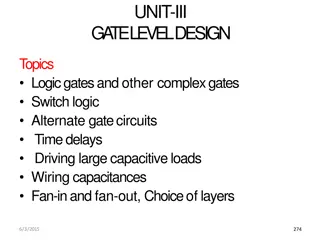
Agenda Last time: Manipulations of Boolean Formulas (3.6) Gates and Combinational Networks (3.7) Incomplete Boolean Functions and Don t Care Conditions (3.8 ) This time: Universal Gates (3.9.3) NAND/NOR/XOR Gate Realizations (3.9.4-3.9.6) Gate Properties (3.10)
Some Terminology System specification: A description of the function of a system and of other characteristics required for its use. A function (table, algebraic) on a finite set of inputs. Double-rail logic: both variables and their complements are considered as primary inputs. Single-rail logic: only variables are considered as primary inputs. Need inverters for their complements.
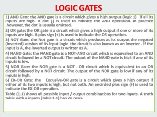
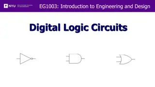
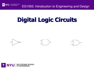
Universal Gates A gate or set of gates is called universal if it can implement all Boolean functions. Standard universal gates: AND, OR, NOT Proof? Theorem: A set of gates ?1, ,?? is universal if it can implement AND, OR, NOT.
NAND is Universal Recall ???? ?,? = ? ? = ? + ? ??? ? = ? = ? + ? = ???? ?,? ??? ?,? = ?? = ? + ? = ??? ? + ? = ??? ???? ?,? = ???? ???? ?,? ,???? ?,? ?? ?,? = ? + ? = ? + ? = ???(?) + ???(?) = ???? ??? ? ,??? ? = ???? ???? ?,? ,???? ?,?
NOR is Universal Recall ??? = ? + ? = ? ? ??? ? = ? = ? ? = ??? ?,? ??? ? = ?? = ? ? = ???(?) ???(?) = ??? ??? ? ,??? ? = ??? ??? ?,? ,??? ?,? ?? ? = ? + ? = ? ? = ??? ? ? = ??? ??? ?,? = ??? ??? ?,? ,??? ?,?
More on Universal Gates Define a 3-input gate ? ?,?,? = ??? + ?? + ??. Show that ? is universal. ??? ? = ? ?,1,1 ??? ?,? = ? ?,??? ? ,0 = ? ?,? ?,1,1 ,0 ?? ?,? = ?(?,0,?)
NAND-Gate Realizations Na ve approach: build network out of AND/OR/NOT gates, use the universal property above to replace each one with several NAND gates. A better approach: manipulate Boolean expression into the form NAND(A, B, . . .,C)
NAND-Gate Realizations Example: ? ?,?,?,? = ?? + ?? ? + ? = (??) [? ?(? + ?)] (??)--already in correct form ??(? + ?) ? + ? = ? ?
NAND-Gate Realizations Only works if highest-order operation is an or- operation. Highest-order operation is the last operation that is performed when the expression is evaluated. What to do? Negate and repeat the procedure for ?. Then note that ? ?1, ,?? = ????(1,?(?1, ,??))
NAND-Gate Realizations ? ?0,?1,?2,?3 = ?3+ ?2+ ?1?0
NOR-Gate Realizations Essentially the same procedure. See Section 3.9.5 in the textbook.
XOR-Gate Realizations Properties of XOR (a) (b) ? ? = ?? + ?? (i) ? ? = ? ? + ?? ? 0 = ? ? 1 = ? (ii) ? ? = 0 ? ? = 1 (iii) ? ? = ? ? ? ? = ? + ? (iv) ? ? = ? ? (v) ? ? ? = ? ? ? (vi) ? ? ? = ?? ?? (vii) ? + ? = ? ? ?? (viii) ? ? = ? + ? ??? ?? = 0 (ix) If ? ? = ? then ? ? = ? ?? ? ? = ? (x)
Gate Properties The two signal values associated with logic-0 and logic-1 are actually ranges of values. If signal value is in some low-level voltage range between ?? ???and ??(???) then it is assigned to logic-0. When a signal value is in some high-level voltage range between ??(???) and ??(???)it is assigned to logic-1.
Noise Margins The minimal signal value that is acceptable as a logic-1 at the input to a gate is different from the minimal logic-1 signal value that a gate produces at its output. Similar situation for ??(???) Manufacturers normally state a ???(???),???(???),???(???),???(???) in gate specifications. Where ???(???)< ???(???)< ???(???),< ???(???)
Noise Margins Consider connecting output of gate to another gate, where noise is induced between the two gates. Noise Gate 1 Gate 2 Worst case low-level noise margin: Any noise less than ???(???) ???(???)does not affect behavior of Gate 2 on a low-level signal. Worst case high-level noise margin: Any noise less than ???(???) ???(???)does not affect behavior of Gate 2 on a high-level signal.
Fan-Out The signal value at the output of a gate is dependent upon the number of gates to which the output is connected. Limitation on number of gates output can connect to. This is known as the fan-out capability of the gate. Manufacturers specify this limitation. Circuits known as buffers serve as amplifiers for this purpose.
Propagation Delays Digital signals to not change nor do circuits respond instantaneously. Limitation to the overall speed of operation associated with a gate. These time delays are called propagation delays. Time required for output signal to change from low- level to high-level is ????. Time required for output signal to change from high- level to low-level is ????. ???? and ????are, in general, not equal. Manufacturers give maximum times in gate specifications. General measure used is the average propagation delay time, ??? ???= 2 ????+????
Power Dissipation Digital circuit consumes power as a result of the flow of currents. Called power dissipation. Desirable to have low power dissipation and low propagation delay times. These two performance parameters are in conflict with each other. Common measure of gate preformance is the product of the propagation delay and the power dissipation of the gate. This is known as the delay-power product.