Basic Computer Organization and Design - Timing and Control
The timing of all registers in a basic computer is governed by a master clock generator, with clock pulses controlling the flip-flops and registers in the system. Two main types of control organization are Hardwired Control and Micro-programmed Control. The former uses digital circuitry like gates and flip-flops while the latter stores control information in a memory. The block diagram of the hardwired control unit includes decoders, a sequence counter, and control logic gates. An instruction cycle in a basic computer involves fetching, decoding, reading effective addresses, and executing instructions.

Download Presentation

Please find below an Image/Link to download the presentation.
The content on the website is provided AS IS for your information and personal use only. It may not be sold, licensed, or shared on other websites without obtaining consent from the author. Download presentation by click this link. If you encounter any issues during the download, it is possible that the publisher has removed the file from their server.
E N D
Presentation Transcript
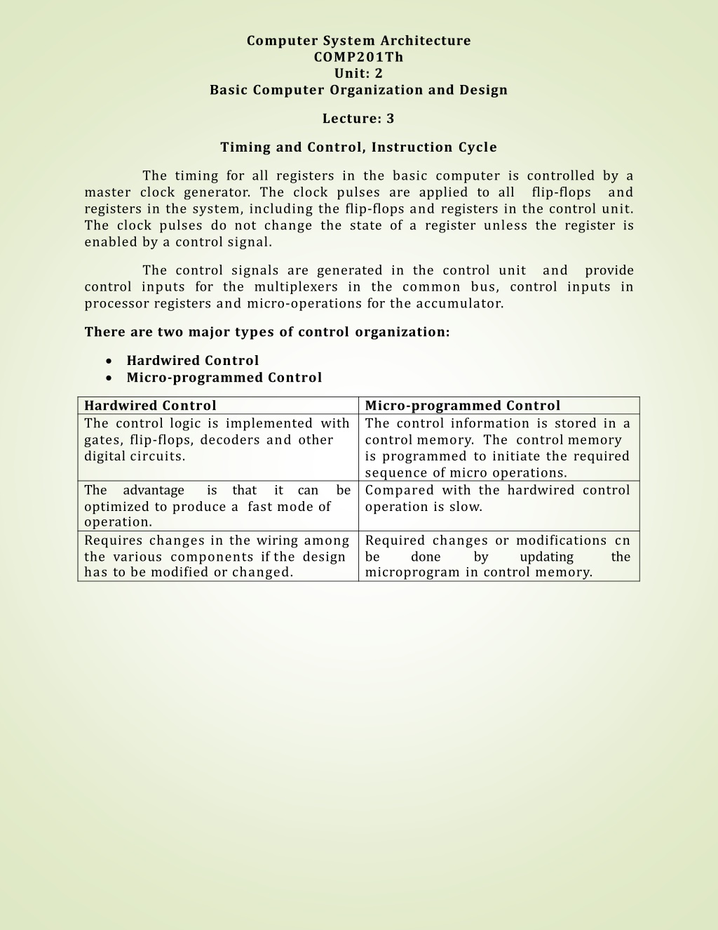
Computer System Architecture COMP201Th Unit: 2 Basic Computer Organization and Design Lecture: 3 Timing and Control, Instruction Cycle The timing for all registers in the basic computer is controlled by a master clock generator. The clock pulses are applied to all registers in the system, including the flip-flops and registers in the control unit. The clock pulses do not change the state of a register unless the register is enabled by a control signal. flip-flops and The control signals are generated in the control unit control inputs for the multiplexers in the common bus, control inputs in processor registers and micro-operations for the accumulator. and provide There are two major types of control organization: Hardwired Control Micro-programmed Control Hardwired Control The control logic is implemented with gates, flip-flops, decoders and other digital circuits. Micro-programmed Control The control information is stored in a control memory. The control memory is programmed to initiate the required sequence of micro operations. Compared with the hardwired control operation is slow. The optimized to produce a fast mode of operation. Requires changes in the wiring among the various components if the design has to be modified or changed. advantage is that it can be Required changes or modifications cn be done by microprogram in control memory. updating the
The block diagram of the hardwired control unit is shown below: Fig: Control Unit of Basic Computer The control unit of basic computers consists of two decoders, a sequence counter and a number of control logic gates. An instruction read from memory is placed in the instruction register (IR). It is divided into three parts: a. The I bit b. The operation code and c. Bits 0 through 11. The operation code in bits 12 through 14 are decoded with a 3*8 decoder. The eight outputs of the decoder are designated by the symbols D0 through D7.
Bit 15 of the instruction is transferred to a flip-flop designated by the symbol I. Bits 0 through 11 are applied to the control logic gates. The 4-bit sequence counter can count in binary from 0 through 15. The outputs of the counter are decoded into 16 timing signals T0 through T15. The sequence counter SC can be incremented or cleared synchronously. The counter is incremented to provide the sequence of timing signals out of the 4*16 decoder. Instruction Cycle: A program residing in the memory unit of the computer consists of a sequence of instructions. The program is executed in the computer by going through a cycle of each instruction. Each instruction cycle in turn is subdivided into a sequence of sub cycles or phases. In the basic computer each instruction cycle consists of the following phases: 1. Fetch an instruction from memory. 2. Decode the instruction 3. Read the effective address from memory if the instruction has an indirect address. 4. Execute the instruction.
Upon the completion of step 4, the control goes back to step 1 to fetch, decode, and execute the next instruction. 1. Fetch instruction: Read instruction code from address in PC and place in IR. (IR Memory[PC]) 2. Decode instruction: Hardware determines what the opcode/function is and determines which registers or memory addresses contain the operands. 3. Fetch operands from the memory if necessary: If any operands are memory addresses, initiate memory read cycles to read them into CPU registers. If an operand is in memory, not a register, then the memory address of the operand is known as the effective address (EA). The fetching of an operand can therefore be denoted as Register Memory[EA]. 4. Execute: Perform the function of the instruction. If arithmetic or logic instruction, utilize the ALU circuits to carry out the operation on data in registers.