Understanding Logic Gates and Large Load Driving in GA-TE Level Design
In GA-TE Level Design, the topics cover logic gates, complex gates, switch logic, gate circuits, timedelays, driving capacitive loads, wiring capacitances, fan-in and fan-out, choice of layers, NMOS and PMOS gate constructions, parasitics and performance impact, strategies for driving large loads, and a summary of StaticCMOS advantages and disadvantages. Various concepts like implementing NAND and NOR functions using NMOS and PMOS devices, understanding the impact of parasitics on performance, and dealing with capacitance when driving large loads are discussed in detail.

Download Presentation

Please find below an Image/Link to download the presentation.
The content on the website is provided AS IS for your information and personal use only. It may not be sold, licensed, or shared on other websites without obtaining consent from the author. Download presentation by click this link. If you encounter any issues during the download, it is possible that the publisher has removed the file from their server.
E N D
Presentation Transcript
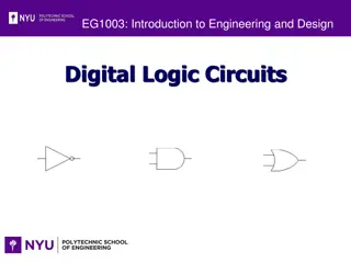
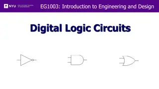
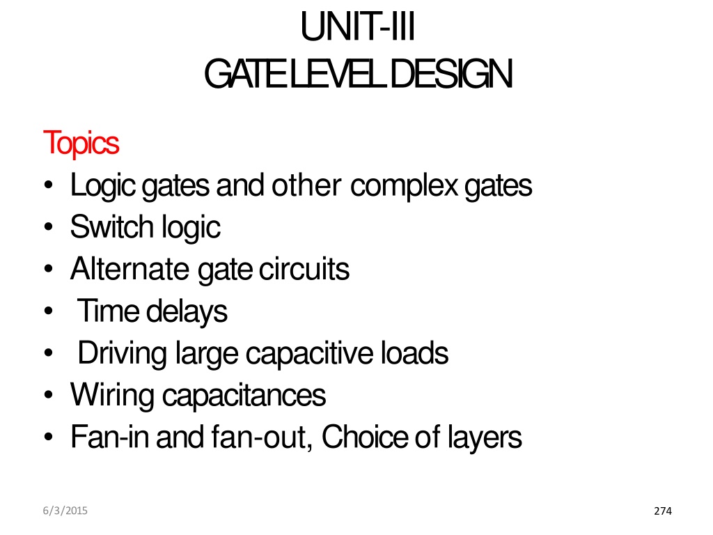
UNIT-III GA TE LEVELDESIGN Topics Logic gates and other complexgates Switchlogic Alternate gatecircuits Timedelays Driving large capacitiveloads Wiringcapacitances Fan-in and fan-out, Choice oflayers 6/3/2015 274
NMOS Gate construction NMOS devices in series implement a NAND function A B A B F A 0 0 1 0 1 1 B 1 0 1 1 1 0 NMOS devices in parallel implement a NOR function A B F A + B 0 0 1 A B 0 1 0 1 0 0 0 1 1 275 6/3/2015
PMOS Gateconstruction PMOS devices in parallel implement a NAND function A B F 0 0 1 A B 0 1 1 1 0 1 A B 1 1 0 PMOS devices in series implement a NOR function A B F 0 0 1 B 0 1 0 A 1 0 0 0 A +B 1 1 276 6/3/2015
Parasitics andPerformance Consider the followinglayout: What is theimpact on performanceof parasitics At point a (VDDrail)? At point b(input)? At Point c(output)? a b c 6/3/2015 277
Parasitics andPerformance a - powersupply connections capacitance -no effect ondelay resistance -increabses delay (see p.135) minimize byreducing difffusionlength minimizeusing parallel vias a c 6/3/2015 278
Driving LargeLoads Off-chip loads, long wires, etc. have highcapacitance Increasing transistor size increases driving ability (and speed), but in turn increases gatecapacitance Solution: stages of progressively largertransistors Use nopt =ln(Cbig/Cg). Scale by a factor of a=e 6/3/2015 281
Summary: StaticCMOS Advantages High Noise Margins (VOH=VDD,VOL=Gnd) No static power consumption (except forleakage) Comparable rise and fall times (with propersizing) Robust and easy to use Disadvantages Large transistor counts (2N transistors for Ninputs) Largerarea More parasitic loading (2 transistor gates on eachinput) Pullupissues Lower driving capability of Ptransistors Series connections especially problematic Sizing helps, but increases loading on gateinputs 6/3/2015 282
Alternatives to StaticCMOS SwitchLogic nmos Pseudo-nmos Dynamic Logic Low-PowerGates 6/3/2015 283
SwitchLogic Key idea: use transistors asswitches Concern: switches arebidirectional A B AND OR 6/3/2015 284
Switch Logic - PassTransistors Use n-transistor as switches Thresholdproblem Transistor switches off when Vgs <Vt VDD input -> VDD-Vtoutput pecial gate needed to restore values IN: VDD OUT: VDD-Vtn A: VDD 6/3/2015 285
Switch Logic - TransmissionGates Complementary transistors - n andp No threshold problem Cost: extra transistor, extra controlinput Not a perfectconductor! A A A A 6/3/2015 286
Switch Logic Example - 2-1MUX IN 6/3/2015 287
ChargeSharing Consider transmission gates in series Each node has parasitic capacitances Problems occur when inputs change to redistribute charge Solution: design network so there is always a path from VDD or Gnd to output 6/3/2015 288
Aside: Transmission Gates inAnalog TransmissionGates work with analog values,too! Example: Voltage-Scaling D/AConverter 6/3/2015 289
NMOSLogic Used before CMOS was widely available Uses only n transistors Normal n transistors inpull- downnetwork depletion-mode ntransistor (Vt < 0) used forpull-up "ratioed logic"required Tradeoffs: Simplerprocessing Smallergates higherpower! Additionaldesign considerations for ratioedlogic Passive PullupDevice: depletion Mode n-transistor (Vt < 0) OUT Pulldown Network 290 6/3/2015
Pseudo-nmosLogic Same idea, as nmos, but use p- transistor forpullup "ratioed logic" required for proper design(more about this next) Tradeoffs: Fewer transistors -> smaller gates,esp.for largenumber of inputs less capacitative load ongates that driveinputs larger powerconsumption less noise margin (VOL >0) additional design considerations due to ratioed logic Passive PullupDevice: P-Transistor OUT Pulldown Network 6/3/2015 291
Rationed Logic for Pseudo-nmos Approach: Assume VOUT=VOL=0.25*VDD Assume 1 pulldown transistor ison Equate currents in p, ntransistors Solve for ratio between sizes of p, n transistors to get theseconditions necessary for Further calculations seriesconnections Idn = Ipn ( 2 2 Idp OUT Pulldown Network Idn 2(V (EQ 3 21) Wp V )2 =1k' V )V Wn 1k' V2 gs,n V nLn pLp tn gs,p tp ds,p ds,p Wp L p 3.9 (EQ 3 22) Assu ming VDD=3.3V WnLn 6/3/2015 292
DCVSLogic DCVS - Differential Cascode VoltageSwitch Differential inputs,outputs Two pulldown networks Tradeoffs Lower capacitativeloading than staticCMOS No ratioed logicneeded Low staticpower consumption More transistors More signals toroute between gates OUT OUT A B C A B C OUT OUT Pulldown Network Pulldown Network 6/3/2015 293
DynamicLogic Key idea: Two-stepoperation precharge - charge C S to logichigh evaluate - conditionally dischargeC S Control - precharge clockf StorageNode CS Precharge Signal Storage Capacitance Pulldown Network B A C Precharge Evaluate Precharge 6/3/2015 294
DominoLogic Key idea: dynamic gate +inverter Cascaded gates - monotonically increasing CS Pulldown Network B C in4 x1 x2 x3 6/3/2015 295
Domino LogicTradeoffs Fewer transistors -> smallergates Lower power consumption thanpseudo-nmos Clockingrequired Logic not complete (AND, OR, but noNOT) 6/3/2015 296