Understanding Combinational Circuits in Digital Electronics
Combinational circuits are an essential component of digital electronics, combining different gates to perform specific functions without memory usage. They provide outputs based solely on present input levels, with no influence from previous states. Types of combinational circuits include half adders for basic binary addition and full adders for more complex operations. Explore the concepts behind combinational circuits and their applications in digital systems.

Download Presentation

Please find below an Image/Link to download the presentation.
The content on the website is provided AS IS for your information and personal use only. It may not be sold, licensed, or shared on other websites without obtaining consent from the author. Download presentation by click this link. If you encounter any issues during the download, it is possible that the publisher has removed the file from their server.
E N D
Presentation Transcript
Arithmetic Circuits
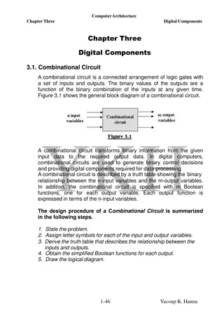
Combinational Circuits Combinational circuit is a circuit in which the different gates are combined in the circuit, for example encoder, decoder, multiplexer and de-multiplexer. Some of the characteristics of combinational circuits are following The output of combinational circuit at any instant of time, depends only on the levels present at input terminals. The combinational circuit do not use any memory. The previous state of input does not have any effect on the present state of the circuit. A combinational circuit can have an n number of inputs and m number of outputs.
Combinational Circuits Block diagram
Combinational Circuits Half Adder Half adder is a combinational logic circuit with two inputs and two outputs. The half adder circuit is designed to add two single bit binary number A and B. It is the basic building block for addition of two single bit numbers. This circuit has two outputs carry and sum. Block diagram Truth Table Circuit Diagram
Combinational Circuits Full Adder Full adder is developed to overcome the drawback of Half Adder circuit. It can add two one-bit numbers A and B, and carry c. The full adder is a three input and two output combinational circuit. Block diagram
Combinational Circuits Truth Table Circuit Diagram
Binary Adder & Subtractor The most basic arithmetic operation is the addition of two binary digits. This simple addition consists of four possible elementary operations: 0 + 0 = 0, 0 + 1 = 1, 1 + 0 = 1, and 1 + 1 = 10. The first three operations produce a sum of one digit, but when both augend and addend bits are equal to 1, the binary sum consists of two digits.
Binary Adder/Subtractors The subtraction A-B can be performed by taking the 2's complement of B and adding to A. The 2's complement of B can be obtained by complementing B and adding one to the result. A-B = A + 2C(B) = A + 1C(B) + 1 = A + B + 1
4-bit Binary Adder/Subtractor ADD/SUB ADD/SUB
4-bit Binary Adder/Subtractor (cont.) When ADD/SUB=0, the circuit performs A + B. The carry in is 0, and the XOR gates simply pass B untouched. When ADD/SUB =1, the carry into the least significant bit (LSB) is 1, and B is complemented (1 s complement) prior to the addition; hence, the circuit adds to A the 1 s complement of B plus 1 (from the carry into the LSB) (or) A - B = A + (2 s complement of B)
4-bit Binary Adder/Subtractor (cont.) S=0 B3 B2 B1 B0 0 S=0 selects addition
4-bit Binary Adder/Subtractor (cont.) S=1 B3 B2 B1 B0 1 S=1 selects subtraction
Binary Codes The digital data is represented, stored and transmitted as groups of binary bits. The group of bits is called as binary code. The binary code represent numbers, alphabets, special characters and control functions. The codes are classified as Weighted codes Non-weighted codes Error detecting and correcting codes Alphanumeric codes
Conversion and Coding (12)10
Conversion and Coding (12)10 1100 Conversion
Conversion and Coding (12)10 Coding (using BCD code for each digit) 00010010 1100 Conversion
BCD Adder Design a circuit that calculates the Arithmetic addition of two decimal digits. 9 3 + 1 2 carry
BCD Adder Maximum sum is 9+9 + 1 = 19 Max digits Carry from previous digits
BCD adder (sum up to 9) Number 0 1 2 3 4 5 6 7 8 9 C 0 0 0 0 0 0 0 0 0 0 S8 0 0 0 0 0 0 0 0 1 1 S4 0 0 0 0 1 1 1 1 0 0 S2 0 0 1 1 0 0 1 1 0 0 S1 0 1 0 1 0 1 0 1 0 1
BCD adder (sum up to 9) Number 0 1 2 3 4 5 6 7 8 9 C 0 0 0 0 0 0 0 0 0 0 S8 0 0 0 0 0 0 0 0 1 1 S4 0 0 0 0 1 1 1 1 0 0 S2 0 0 1 1 0 0 1 1 0 0 S1 0 1 0 1 0 1 0 1 0 1 The sum is the same with BCD adder
BCD adder (sum is 10 to 19) Number 10 11 12 13 14 15 16 17 18 19 C 1 1 1 1 1 1 1 1 1 1 S8 0 0 0 0 0 0 0 0 1 1 S4 0 0 0 0 1 1 1 1 0 0 S2 0 0 1 1 0 0 1 1 0 0 S1 0 1 0 1 0 1 0 1 0 1
BCD adder (sum is 10 to 19) Binary sum BCD adder sum C 1 1 1 1 1 1 1 1 1 1 S8 0 0 0 0 0 0 0 0 1 1 S4 0 0 0 0 1 1 1 1 0 0 S2 0 0 1 1 0 0 1 1 0 0 S1 0 1 0 1 0 1 0 1 0 1 Number K 0 0 0 0 0 0 1 1 1 1 Z8 1 1 1 1 1 1 0 0 0 0 Z4 0 0 1 1 1 1 0 0 0 0 Z2 1 1 0 0 1 1 0 0 1 1 Z1 0 1 0 1 0 1 0 1 0 1 10 11 12 13 14 15 16 17 18 19
BCD adder (sum is 10 to 19) Binary sum BCD adder sum C 1 1 1 1 1 1 1 1 1 1 S8 0 0 0 0 0 0 0 0 1 1 S4 0 0 0 0 1 1 1 1 0 0 S2 0 0 1 1 0 0 1 1 0 0 S1 0 1 0 1 0 1 0 1 0 1 Number K 0 0 0 0 0 0 1 1 1 1 Z8 1 1 1 1 1 1 0 0 0 0 Z4 0 0 1 1 1 1 0 0 0 0 Z2 1 1 0 0 1 1 0 0 1 1 Z1 0 1 0 1 0 1 0 1 0 1 10 11 12 13 14 15 16 17 18 19
BCD adder (sum is 10 to 19) Binary sum BCD adder sum C 1 1 1 1 1 1 1 1 1 1 S8 0 0 0 0 0 0 0 0 1 1 S4 0 0 0 0 1 1 1 1 0 0 S2 0 0 1 1 0 0 1 1 0 0 S1 0 1 0 1 0 1 0 1 0 1 Number K 0 0 0 0 0 0 1 1 1 1 Z8 1 1 1 1 1 1 0 0 0 0 Z4 0 0 1 1 1 1 0 0 0 0 Z2 1 1 0 0 1 1 0 0 1 1 Z1 0 1 0 1 0 1 0 1 0 1 10 11 12 13 14 15 16 17 18 19 +6
Algorithm for BCD Adder Add two numbers using ordinary binary addition. If sum is equal to or less than 9, no correction is needed and the sum is in correct BCD form. Use the regular Adder. If the sum > 9 or if carry is generated from the result, the result is invalid and the correction is needed. Use the regular adder and add 6 (0110) to the result
BCD Adder
Data Processing Circuits Multiplexers & De-Multiplexers
MULTIPLEXERS A multiplexers (MUX) is a device that allows digital information from several sources to be routed onto a single line for transmission that line to a common destination. The basic multiplexers has several data input lines and a single output line. MUX is also called as data selector because the output bit depends on the input data bit that is selected. 32
8x1 Multiplexer F A B C 0 0 0 0 0 1 I0 I1 I2 I3 I4 I5 I6 I7 0 1 0 0 1 1 1 0 0 1 0 1 1 1 0 1 1 1 MSB LSB Z = A .B'.C'.I0 + A'.B'.C.I1 + A'.B.C'.I2 + A'.B.C.I3 + A.B'.C'.I0 + A.B'.C.I1 + A'.B.C'.I2 + A.B.C.I3 37
Demultiplexers De-multiplexer means one into many . It is a combinational logic circuit with one input and many outputs. A demultiplexer has 1 data input, N control inputs, 2N outputs A demultiplexer routes (or connects) the data input to the selected output. The value of the control inputs determines the output that is selected. A demultiplexer performs the opposite function of a multiplexer. 39
De-multiplexers W X Y Z W = A'.B'.I Out0 Out1 Out2 Out3 X = A.B'.I I In Y = A'.B.I S1 S0 Z = A.B.I A B W X Y Z A B 0 0 I 0 0 0 0 1 0 I 0 0 1 0 0 0 I 0 1 1 0 0 0 I 41
Decoders 42
Decoders Decoder is a combinational circuit that decodes the information on N input lines to a max. of 2N output lines A decoder is a logic circuit that accepts a set of inputs that represents a binary number and activates only the output that corresponds to the input number. In other words, a decoder circuit looks at its inputs, determines which binary number is present there, and activates the one output that corresponds to that number ; all other outputs remain inactive. A decoder has N inputs & 2N outputs A decoder selects one of 2N outputs by decoding the binary value on the N inputs. Converting from Binary to Decimal is called Decode. 43
Decoders W = A'.B' W X Y Z Out0 Out1 Out2 Out3 X = A.B' B A I0 I1 Y = A'.B Z = A.B msb Active-high outputs W X Y Z A B 0 0 1 0 0 0 0 1 0 1 0 0 1 0 0 0 1 0 1 1 0 0 0 1 44
Decoders W = (A'.B')' W X Y Z Out0 Out1 Out2 Out3 X = (A.B')' B A I0 I1 Y = (A'.B)' Z = (A.B)' msb Active-low outputs W X Y Z A B 0 0 0 1 1 1 0 1 1 0 1 1 1 0 1 1 0 1 1 1 1 1 1 0 45
Decoders msb Fall 2010 ECE 331 - Digital System Design 46
Decoder with Enable W X Y Z Out0 Out1 Out2 Out3 B A I0 high-level enable I1 Enable En W X Y Z En A B 1 0 0 1 0 0 0 1 0 1 0 1 0 0 enabled 1 1 0 0 0 1 0 1 1 1 0 0 0 1 0 x x 0 0 0 0 disabled Fall 2010 ECE 331 - Digital System Design 47
Decoder with Enable W X Y Z Out0 Out1 Out2 Out3 B A I0 low-level enable I1 Enable En W X Y Z En A B 0 0 0 1 0 0 0 0 0 1 0 1 0 0 enabled 0 1 0 0 0 1 0 0 1 1 0 0 0 1 1 x x 0 0 0 0 disabled Fall 2010 ECE 331 - Digital System Design 48
Decoder Decoders are used in many types of applications. One example is in computers for I/O selection. Computer must communicate with a variety of external devices called peripherals by sending and/or receiving data through what is known as input/output (I/O) ports Each I/O port has a number, called an address, which uniquely identifies it. When the computer wants to communicate with a particular device, it issues the appropriate address code for the I/O port to which that particular device is connected. The binary port address is decoded and appropriate decoder output is activated to enable the I/O port. Binary data are transferred within the computer on a data bus through a set of parallel lines. 49
Encoders 50


")
")
")


")
")
")
")
")
")