Understanding the Basics of Multi-Stage Architecture in CPU Design
The article explains the fundamentals of a multi-stage digital processing system in computer organization, focusing on the central processing unit (CPU). It covers topics such as instruction execution, processor building blocks, and the benefits of pipelined operation. Concepts like fetching, decoding, executing instructions, and memory access are elaborated with visual aids. The role of control circuitry, ALU, and register files in CPU operation is highlighted, emphasizing the pipelined organization for high-performance processors.

Uploaded on Oct 06, 2024 | 0 Views
Download Presentation

Please find below an Image/Link to download the presentation.
The content on the website is provided AS IS for your information and personal use only. It may not be sold, licensed, or shared on other websites without obtaining consent from the author. Download presentation by click this link. If you encounter any issues during the download, it is possible that the publisher has removed the file from their server.
E N D
Presentation Transcript
SISTEMI EMBEDDED Computer Organization Central Processing Unit (CPU) Last version: 20180515 Federico Baronti
Processing Unit A processor reads program instructions from the computer s memory and executes them. This includes the following basic phases: Fetching and decoding the instruction Executing the instruction, which includes: 1. Reading one or more registers (in the register file) 2. Doing some computation (in the ALU) 3. Accessing the memory 4. Writing a register (in the register file) datapath
Processors building blocks PC provides instruction address Instruction is fetched into IR Instruction address generator updates PC ALU performs some computation during execution Control circuitry interprets instruction and generates control signals to perform the actions needed.
A digital processing system datapath
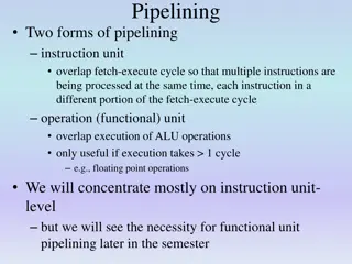
Why multi-stage? Processing moves from one stage to the next in each clock cycle Such a multi-stage system is the basis for pipelined operation High-performance processors have a pipelined organization Pipelining enables the execution of successive instructions to be overlapped We will get back to pipeline later. Let s now focus on the basics of the multi-stage architecture of a RISC-style processor
Instruction execution Pipelined organization is most effective if all instructions can be executed in the same number of steps. Each step is carried out in a separate hardware stage. Processor design will be illustrated using five hardware stages. How can instruction execution be divided into five steps? Let s start from some representative RISC instructions
A memory access instruction: Load R5, X(R7) 1. Fetch the instruction and increment the program counter. 2. Decode the instruction and read the contents of register R7 in the register file. 3. Compute the effective address = X + [R7]. 4. Read the memory source operand. 5. Load the operand into the destination register, R5.
A computational instruction: Add R3, R4, R5 1. Fetch the instruction and increment the program counter. 2. Decode the instruction and read registers R4 and R5. 3. Compute the sum [R4] + [R5]. 4. No action. 5. Load the result into the destination register, R3. Stage 4 (memory access) is not involved in this instruction.
5-stage Architecture of a RISC Processor 1. Fetch an instruction and increment the program counter. 2. Decode the instruction and read registers from the register file. 3. Perform an ALU operation. 4. Read or write memory data if the instruction involves a memory operand. 5. Write the result into the destination register. This sequence determines the hardware stages needed.
Hardware components: Register file A 2-port register file is needed to read the two source registers at the same time. It may be implemented using a 2-port memory.
Hardware components: ALU (1) Both source operands and the destination location are in the register file. [RA] and [RB] denote values of registers that are identified by addresses A and B [RB] new [RC] [RA] new [RC] denotes the result that is stored to the register identified by address C
Hardware components: ALU (2) In this case, one of the source operands is the immediate value in the IR. new [RC] [RA]
A 5-stage implementation of a RISC processor Instruction processing moves from stage to stage in every clock cycle, starting with fetch. The instruction is decoded and the source registers are read in stage 2. Computation takes place in the ALU in stage 3.
A 5-stage implementation of a RISC processor If a memory operation is involved, it takes place in stage 4. The result of the instruction is written in the destination register in stage 5.
The datapath Stages 2 to 5 Register file, used in stages 2 and 5 (Inter-stage registers RA, RB, RZ, RM, RY needed to carry data from one stage to the next) ALU stage Memory stage Final stage to store result to the register file
Memory stage For a calculation instruction: MuxY selects [RZ] to be placed in RY. For a memory instruction: RZ provides memory address, and MuxY selects read data to be placed in RY. RM provides data for a memory write operation. In subroutine calls or exception handling: Input 2 of MuxY is used (return address stored in the register file)
Instruction Fetch Stage (1) MuxMA selects the PC when fetching instructions (RZ in the Memory Stage we are assuming no Harvard architecture) The Instruction address generator increments the PC after fetching an instruction It also generates branch and subroutine addresses.
Instruction Fetch Stage (2) When an instruction is read, it is placed in IR. The control circuitry decodes the instruction. It generates the control signals that drive all units. The Immediate block extends the immediate operand to 32 bits, according to the type of instruction.
Instruction address generator Connections to registers RY and RA are used to support subroutine call and return instructions
Example: Add R3, R4, R5 1. Memory address [PC], Read memory, IR Memory data, PC [PC] + 4 2. Decode instruction, RA [R4], RB [R5] 3. RZ [RA] + [RB] 4. RY [RZ] 5. R3 [RY]
Example: Load R5, X(R7) 1. Memory address [PC], Read memory, IR Memory data, PC [PC] + 4 2. Decode instruction, RA [R7] 3. RZ [RA] + Immediate value X 4. Memory address [RZ], Read memory, RY Memory data 5. R5 [RY] = X
Example: Store R6, X(R8) 1. Memory address [PC], Read memory, IR Memory data, PC [PC] + 4 2. Decode instruction, RA [R8], RB [R6] 3. RZ [RA] + Immediate value X, RM [RB] 4. Memory address [RZ], Memory data [RM], Write memory 5. No action
Unconditional branch 1. Memory address [PC], Read memory, IR Memory data, PC [PC] + 4 2. Decode instruction 3. PC [PC] + Branch offset 4. No action 5. No action
Conditional branch: Branch_if_[R5]=[R6] LOOP 1. Memory address [PC], Read memory, IR Memory data, PC [PC] + 4 2. Decode instruction, RA [R5], RB [R6] 3. Compare [RA] to [RB], If [RA] = [RB], then PC [PC] + Branch offset 4. No action 5. No action
Subroutine call with indirection: Call_register R9 1. Memory address [PC], Read memory, IR Memory data, PC [PC] + 4 2. Decode instruction, RA [R9] 3. PC-Temp [PC], PC [RA] 4. RY [PC-Temp] 5. Register LINK [RY]
Control signals Select multiplexer inputs to route the flow of data Set the function performed by the ALU Determine when data are written into the PC, the IR, the register file, and the memory
Register file control signals Generated by decoding the OPCODE field of the instruction hold in the IR register Instruction Format R I
ALU control signals Generated by decoding the OPCODE field of the instruction hold in the IR register Analyzed by the CONTROL CIRCUITRY during the execution of a branch instruction
Result selection Generated by decoding the OPCODE field of the instruction hold in the IR register
Memory access When data are found in the cache, access to memory can be completed in one clock cycle. Otherwise, read and write operations may require several clock cycles to load data from main memory into the cache. A control signal is needed to indicate that memory function has been completed (MFC). E.g., for step 1: 1.Memory address [PC], Read memory, Wait for MFC, IR Memory data, PC [PC] + 4
Memory and IR control signals 1. Imm 16-bit sign extended 2. Imm 16-bit unsigned extended 3. Imm 16-bit high extended 4. Imm 26-bit in CALL instr. which is special extended MuxY
Control signals of instruction address generator
Control signal generation Circuitry must be implemented to generate control signals so actions take place in correct sequence and at correct time. There are two basic approaches: hardwired control and microprogramming Hardwired control involves implementing circuitry that considers step (ring) counter, IR, ALU result, and external inputs. Step (Ring) counter keeps track of execution progress, one clock cycle for each of the five steps described (unless a memory access takes longer than one cycle).
Hardwired generation of control signals E.g. RF_wtite = T5&(ALU | Load | Call); PC_enable = T1&MFC | T3&(BR | Ret | Call);
CISC processors CISC-style processors have more complex instructions. The full set of instructions cannot all be implemented in a fixed number of steps. Execution steps for different instructions do not all follow a prescribed sequence of actions. Hardware organization should therefore enable a flexible flow of data and actions to accommodate CISC.
Hardware organization for a CISC computer Main difference between 5-stage RISC organization and CISC organization, where a datapath cannot be identified easily Hold temporary results during instruction execution
Bus An example of an interconnection network. When functional units are connected to a common bus, tri-state drivers are needed. Register Enable
A 3-bus interconnection network Example 1: Add R5, R6 1. Memory address [PC], Read memory, Wait for MFC, IR Memory data, PC [PC] + 4 2. Decode instruction 3. R5 [R5] + [R6]
A 3-bus interconnection network Example 2: And X(R7), R9 1. Memory address [PC], Read memory, Wait for MFC, IR Memory data, PC [PC] + 4 Decode instruction Memory address [PC], Read memory, Wait for MFC, Temp1 Memory data, PC [PC] + 4 Temp2 [Temp1] + [R7] Memory address [Temp2], Read memory, Wait for MFC, Temp1 Memory data Temp1 [Temp1] AND [R9] Memory address [Temp2], Memory data [Temp1], Write memory, Wait for MFC 2. 3. 4. 5. 6. 7. X is stored as a second word of the instruction
References C. Hamacher, Z. Vranesic, S. Zaky, N. Manjikian "Computer Organization and Embedded Systems, McGraw-Hill International Edition Chapter V: Basic Processing Unit


")
")


")
")


")
")