Insights into Current Mirror Frequency Response
The frequency response of a current mirror involves poles and zeros, where the zero can impact phase similar to the pole. The combined pole and zero contribute to an overall phase change of 180 degrees, influencing the mirror's behavior.

Download Presentation

Please find below an Image/Link to download the presentation.
The content on the website is provided AS IS for your information and personal use only. It may not be sold, licensed, or shared on other websites without obtaining consent from the author. Download presentation by click this link. If you encounter any issues during the download, it is possible that the publisher has removed the file from their server.
E N D
Presentation Transcript
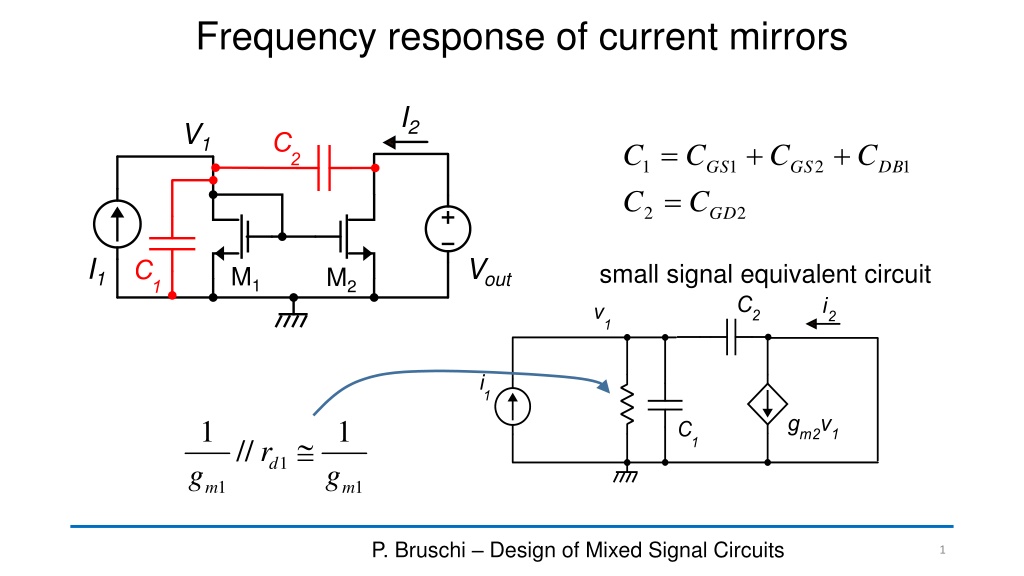
Frequency response of current mirrors I2 V1 = + + C C C C 1 1 2 1 GS GS DB = C C 2 2 GD I1 Vout small signal equivalent circuit M1 M2 1 1 // r 1 d g g 1 1 m m P. Bruschi Design of Mixed Signal Circuits 1
Small signal equivalent circuit ( ) s Z in ( ) = = v g sC i g v sC v 1 2 2 2 2 1 ( ) s i 2 1 m m = v Z 1 1 in 1 ( ) s = Z ( ) in + + g s C C g + sC 1 1 2 m = 2 s C 2 m i i ( ) 2 1 + g g C = 1 C m 1 1 2 m s p + C 1 1 2 C g g C 0 1 s 2 = = (0) A A z 2 m g g i i ( ) I I s z = = 2 2 C m m + A s 2 + ( ) 1 2 = I C g g ( ) + 1 2 1 2 m A 1 1 s m p I g 1 m 1 m P. Bruschi Microelectronic System Design 2
Frequency response of the current gain AI g C C + g C = s 1 m W L ( ) 1 = p g C V V I A m OX GS t 1 2 = (0) A A z dB I I s + 1 = 2 m ) 0 ( IA z fz fp p 2 log(f) / / g g W W L L ( ) IA ( ) 0 = = = 2 k m 2 2 A M I 1 1 1 m g g g C g IA ( ) = ( ) 0 = 2 1 C m m A A 2 P ( ) log(f) I I + C 1 1 2 2 Z m m -90 C + ( ) = 1 A 2 I C C -180 1 2 P. Bruschi Microelectronic System Design 3
Frequency response of current mirrors with AI<<1 I A / / g g W W L L ( ) 0 dB fp fz = 2 m A k 2 2 I M 1 1 1 m log(f) ( IA ) ( ) 0 If 1 IA ) 0 ( IA we can expect that: C + ( ) 0 ( ) = IA A A 2 I I C C log(f) 1 2 -90 -180 P. Bruschi Microelectronic System Design 4
Upper band limit (fH) of a current mirror C2 I2 Hypothesis: fp<fzthen: fH=fp V1 Vout M1 M2 I1 C1 g 1 C C g g = p = 1 + m 1 m C 1 m C f ( ) p 2 2 2 2 C C 1 gs 1 1 2 gs gs 2 gs + 1 neglecting CDB1in C1 Tf 1 gs 1 2 3 2 3 f C C W L = f 1 T C C f W L W L 2 2 2 gs OX p f 1 T p 2 gs + 1 + 1 2 2 C C W L 1 gs 1 1 1 gs OX 1 1 P. Bruschi Microelectronic System Design 5
Upper band limit (fH) of a current mirror f W L W L In strong inversion = = f f 1 T 3 1 L H p ( ) = f V V + 1 2 2 T GS t 2 1 4 1 1 Fast current mirrors: Short channel length Large overdrive voltage (VGS-Vt) Precision current mirror: f f 1 T k / / W L W L W W W W L L ( ) = = = = 2 2 2 2 2 L L k p + 1 1 2 M M 1 1 1 1 1 P. Bruschi Microelectronic System Design 6
Summary 1. The frequency response of a current mirror is marked by a pole (angular frequency p) and a zero (angular frequency z). 2. The zero (sz) is positive, then it gives a phase contribution similar to that of the pole. In total, the pole and zero give an asymptotic phase variation of 180 . 3. Generally, the pole falls at lower frequencies than the zero, thus the upper band limit is given by the pole. 4. The frequency of the zero is smaller than the pole frequency only for mirrors designed to have a current gain << 1. 5. In all other cases, which include unity gain current mirrors, the upper band limit is given by: 1 T H p f f W L W L f = = + 1 2 2 1 1 P. Bruschi Microelectronic System Design 7
Noise in current mirrors Simple MOSFET current mirror 2 = = = + n out i i i A i ( ) f ( ) f ( ) ( ) f S S A f S 2 1 Iout In I In 2 2 1 n I n ( ) 0 A A For f << fH I I 2 g g 2 = + ( ) f ( ) f ( ) f 2 m = + S S S ( ) f ( ) f (0) ( ) f S S A S 2 1 Iout In In 2 1 Iout In I In 1 m P. Bruschi Microelectronic System Design 8
Thermal noise Let us assume: 8 3 8 3 8 3 = ( ) f S kTg = ( ) f S kTg 1 1 In Th m In Th m g g = ( ) f S kTg ( ) 0 = = 2 m A k 2 2 In Th m I M 1 m 2 g g = + 2 m ( ) f ( ) f ( ) f 2 m S S S 8 3 8 3 g g = + 2 1 Iout In In ( ) f 2 S kTg kTg 2 1 Iout th m m 2 m 1 m kM 1 8 3 8 3 g g 8 3 ( ) = + ( ) f 2 m S kTg kTg = + ( ) f 1 S kTg k 2 2 Iout th m m 2 Iout th m M 1 m P. Bruschi Microelectronic System Design 9
Flicker Noise Let us assume: N 1 f = 2 m ( ) f S g 1 1 In F N WL f W L f 1 f = 2 m 1 1 ( ) f S g In F N 1 f = 2 m ( ) f S g 1 2 In F W L f 2 2 2 N N 2 m g g 1 1 g g f f = + = + 2 m 2 m ( ) f 2 S g g ( ) f ( ) f ( ) f 2 m S S S 2 1 Iout F 2 1 Iout In In 2 m W L f W L f 2 2 1 1 1 1 m N N 1 1 N 1 f W L W L f f = + 2 m 2 m ( ) f S g g f = + 2 m ( ) f 1 S g 2 2 2 2 Iout F W L f W L f 2 Iout F W L 2 2 1 1 2 2 1 1 P. Bruschi Microelectronic System Design 10
Parameters that affect the output noise 8 3 ( ) = + ( ) f 1 S kTg k Thermal noise: 2 Iout th m M N 1 f W L W L f = + 2 m ( ) f 1 S g 2 2 Flicker noise: In F 2 W L 2 2 1 1 8 3 I The higher the current ID2, the higher the output current PSD High values of VTE reduce noise ( ) = + ( ) f 1 S kT k 2 D Iout th M V I 2 TE N = g D Using: 2 m 1 f I W L W L V f = + ( ) f 1 S 2 2 2 D TE In F V W L 2 2 2 1 1 TE P. Bruschi Microelectronic System Design 11
Dynamic range of a current mirror = = + ( ) t I I out i out out Q = + 1( ) i t I I out FS i i 1 1 Q = DR out n dc bias = out i I signal FS 2 out Q Iout For simplicity, let us consider a sinusoidal stimulus iout-FS = Iout-Q 2 2 I I peak out Q Ipeak =2 only if we allow the minimum value of Ioutto be zero -> distortion t P. Bruschi Microelectronic System Design 12
DR of a current mirror ( ) 2 = out i I FS out Q out FS i i = DR ( ) f f = = H 4 4 np i i S df out n p n rms Iout f L 2 2 out Q I Thermal 16 S B 2 2 out Q I IBB S ( ) 2 = DR f ( ) f df H 2 2 out Q 16 S I Iout f Flicker L f f 16 ln k H F L P. Bruschi Microelectronic System Design 13
DR of a current mirror 2 8 3 I N 1 f I W L W L ( ) = + ( ) f 1 S kT k 2 D f = + ( ) f 1 S 2 2 2 D In F Iout th M V V W L 2 2 2 1 1 TE 2 TE SIBB = I I kf 2 D out Q Thermal: 2 V I 3 2 2 out Q I ( ) 2 TE out Q k + = 2 = DR ( ) I 128 1 kT B 8 3 ( ) out Q V + 16 1 kT k B S M M S 2 TE Flicker: 2 2 out Q 2 2 I V W L W L W L ( ) 2 = = 2 2 2 TE DR 2 I N W L W L f f + out Q V f + 16 1 ln 16 1 ln( / ) N f f 2 2 H 2 2 f H L W L 2 2 2 1 1 TE L 1 1 P. Bruschi Microelectronic System Design 14
Examples Thermal 2 V I 3 2 TE out Q k + = DR ( ) 128 1 kT B S M DR (88 dB, 14 bit) 3 25.7 10 = = = = 1 A I out Q V k B 100 mV 1, 1kHz 2 TE = 1.5 M S P. Bruschi Microelectronic System Design 15
Examples Flicker 2 2 V W L W L W L = DR 2 2 2 TE + 16 1 ln( / ) N f f 2 2 f H L 1 1 DR 319 = = = = 1 A I out Q V k B = = 2 1 m N WL N (50 dB, 8 bit) 100 mV 1, 1kHz 2 TE 6 10 = 10 2 2 m V = 1.5 f fn M Flicker noise dominates This is the total DR = 0.01 Hz f L S P. Bruschi Microelectronic System Design 16


 of a current mirror")
 of a current mirror")