Techniques to Increase Gain in a Simple Differential Amplifier
Explore methods to boost the gain of a simple CMOS differential amplifier by replacing the current mirror with a cascode mirror, adding a common-gate stage, and employing a cascode differential amplifier. These techniques help improve Rout without extensive use of long MOSFETs, optimizing the amplifier's performance.

Download Presentation

Please find below an Image/Link to download the presentation.
The content on the website is provided AS IS for your information and personal use only. It may not be sold, licensed, or shared on other websites without obtaining consent from the author. Download presentation by click this link. If you encounter any issues during the download, it is possible that the publisher has removed the file from their server.
E N D
Presentation Transcript
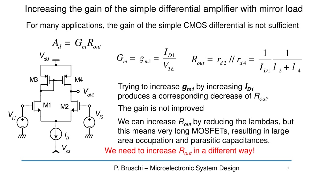
Increasing the gain of the simple differential amplifier with mirror load For many applications, the gain of the simple CMOS differential is not sufficient = A G R d m out I V 1 1 + = = G g 1 D = // = R r r 1 m m 2 4 out d d I l l TE 1 2 4 D Trying to increase gm1by increasing ID1 produces a corresponding decrease of Rout. The gain is not improved We can increase Routby reducing the lambdas, but this means very long MOSFETs, resulting in large area occupation and parasitic capacitances. We need to increase Routin a different way! P. Bruschi Microelectronic System Design 1
Fist step: replace the simple current mirror with a cascode mirror This increases Rup ( ) R r g r up d m d 2 down R r d but Rdownis not changed R r @ 2 out d Routpasses from rd/2 to rdand the gain is only doubled P. Bruschi Microelectronic System Design 2
Second step: add a common-gate also to the differential pair: The cascode differential amplifier ( ) @ 2 + 1 + 2 down R r r g r 2 4 4 2 d d m d 2rd2 We add a differential common gate stage (M3,M4) to the differential pair: forming a differential cascode stage P. Bruschi Microelectronic System Design 3
Cascode differential amplifier: Rout Also in this amplifier, the current into Rdownis brought back to the output ( ) ( ) @ r r g @ + 1 + R r r r g 5 8 5 d d m 8 5 8 5 up d d d m ( ) ( ) @ 2d r r g 2 1 2 down R r r g r @ + + 4 2 4 d m 2 4 4 2 d d m d v R v R The current into Rdownis doubled p p = + 2 i up p down R down R up down R = // R R out up 2 ( ) ( ) @ // R r r g r r g 5 8 5 4 2 4 out d d m d d m P. Bruschi Microelectronic System Design 4
Cascode differential amplifier @ - @ I I I g v 1 2 G v 1 OCC D D m d = I u t OCC m d I-to-I network = = G A g G R ) ( / / 1 m m d m out t ( ) @ A g r g r r g r 1 2 4 4 8 5 5 d m d m d d m d t u If all devices have the same rdand gm: 2 ( ) g r Cascode Differential stage m d A @ d 2 V-to-I network P. Bruschi Microelectronic System Design 5
CMOS cascode amplifier: output range Upper limit out mirror V - V V MIN cascode V - V = - dd out |Vout-mirror| V MIN cascode V - - dd out ( ) max = - V V MIN cascode V - out dd As Voutgets higher than max(Vout), Rup decreases making the gain decrease P. Bruschi Microelectronic System Design 6
CMOS cascode amplifier: output range Lower limit V V V V V DSAT V = - 4 = 4 4 DS out - S V V V V 4 2 4 S k GS DSAT V V - + ) 2 4 4 out min k GS V ( = - + V DSAT V 2 4 4 out k GS ( ) min = - V V V In strong inversion: 2 4 out k t For an approximation of min(Vout) in weak inversion just add 100 mV P. Bruschi Microelectronic System Design 7
Input common mode range ( ) min iC V = V V = - + + V MIN tail V V V - 1 SS GS V 1 1 1 1 DS D S DSAT = = - V V V V V V 1 2 3 D k GS - 1 1 S iC GS V V V V DSAT V - - + 2 3 1 1 k GS iC GS VC VC ( ) iC V max = - + - V V V DSAT V 2 3 1 1 k GS GS ( ) iC V max @ - V DSAT V 2 1 k P. Bruschi Microelectronic System Design 8
Cascode amplifier: all ranges Vout Vdd Vdd max(Vout)=Vdd |VMIN-cascode| max(ViC)=Vk2 VDSAT1 Vout Vk2 Vic min(Vout)=Vk2 VGS4+VDSAT4 Vk2determines a trade- off between the input common mode range and the output swing min(ViC)=VSS +VMIN-tail+VGS1 Vss Vss P. Bruschi Microelectronic System Design 9
Adaptive Vk2 V V V V DSAT V - - + 2 3 1 1 k GS iC GS V V V V DSAT V - + + 2 1 3 1 k iC GS GS V + 1 V S = + V V DSAT V 2 1 3 1 k S GS = + V V V 2 1 10 k S GS = + V V DSAT V 10 3 1 GS GS P. Bruschi Microelectronic System Design 10
Adaptive Vk2 Same as in the case of a general cascode structure = + V V DSAT V 10 3 1 GS GS ) 10 ( ( ) - = + - V V mV V V 3 1 GS t DSAT GS t 3 = - I I I 0 - 0 eff B The adaptive Vk2does not solve the problem that, as ViCincreases, the output swing gets smaller. The advantage is that the amplifier is more flexible and no trade-off on VK2should be made in the design phase. T P. Bruschi Microelectronic System Design 11
Removing the interaction between input and output range: The Folded Cascode Two current sources are required to bias the common source and common gate Folding Let us introduce a type-p common gate stage out According to the folding mechanism, the signal (variations) initially travels from one rail to the other and then invert direction and goes back to the initial rail Use an n-type current mirror to subtract the currents P. Bruschi Microelectronic System Design 12
Folded cascode amplifier: device currents Condition: = = - - I I I I I I 0 0 I I 6 1 2 D D 6 D 7 1 1 D D 7 D = - @ - I I I I I 7 9 7 6 OCC D D D ) ( - D ( ) = - - I I I I I 1 1 1 2 OCC D D = - V V V 1 2 D i i ( ) @- g v = - - I I I 1 m d 1 2 OCC D D P. Bruschi Microelectronic System Design 13
Folded cascode: setting the correct I1value with: I = I Quiescent point: 0 0 I I I I I I = = - - 1 0 6 1 2 D D I I = = 0 I I I 0 1 2 D D 2 7 1 1 D D 2 I > 0 1 2 I I With a large input signal (|Vid|> VDMAX): V V V V < - 0 0 2 2 > : = I I 1 I 0 id DMAX D : = I 2 0 id DMAX D usually: I = I I I 1 0 1 0 P. Bruschi Microelectronic System Design 14
Folded cascode: differential mode gain Using a Norton equivalent circuit of the output port occ i v = = A G R G d m out m rd4 rd3 d Vk2 I g v = - G g @- A = - M7 M6 1 1 OCC m d m m ip g R 1 d m out vp M8 M9 M1 v i M2 p = R out M10 M11 ros p P. Bruschi Microelectronic System Design 15
Folded cascode: output resistance (2) (1) 1 p (2) 1 p ( p 1) (2) 2 p = + = + i i i i i i 1 2 2 p p rd4 rd3 = v v 1 p p = 0 v 1 p = 0 v 2 p = v v Vk2 M7 M6 2 p p ip1 vp1 ip2 M8 vp2 M1 M2 M9 = = v v v 1 = 2 p p p M10 M11 + i i i ros 1 2 p p p P. Bruschi Microelectronic System Design 16
Folded cascode: output resistance (2) v i R (1) 1 ( ) p @ 1 + = / /2 R r g R R r r (1) 1 p = 7 7 7 7 3 1 up d m S S d d ) 1 up ( @ / /2 R r g r r RS7 pi 7 7 3 up d m d d 2rd1 r + (1) 1 p (1) 1 p - = 3 d i i r (1) 1 2 r r pi (1) 1 p i 3 1 d d Rup - r (1) pi 2 r + (1) p (1) 1 p (1) 1 p = = 3 d i i i 2 - r 2 r r ros 3 1 d d P. Bruschi Microelectronic System Design 17
Folded cascode: output resistance (2) @ R r g r 9 9 11 dw d m d v R p (2) 2 p = i dw (2) 1 = 0 v R pi (2) 1 pi p Rdw (1) 1 p = i (2) 2 pi up r + (1) p (1) 1 p = 3 d i i 2 2 r r 3 1 d d ros v R v R r + p p = 1 + + 3 d i p 2 r r 3 1 up d d dw P. Bruschi Microelectronic System Design 18
Folded cascode: output resistance (3) - 1 1 1 r + = 1 + + 3 d i v p p 2 R r r R 1 1 = + R 3 1 up d d dw out R R up r + dw - 1 1 + 3 d 1 1 r + 2 r r = 1 + + 3 2 d R 3 1 d d out R r r R 3 2 up d d dw If rd2=rd3=rd7=rd9=rd11=rd gm7=gm9=gm = / / R R up r R ( r g r ) = R r g r 2 3 - out dw dw d m d ( 2 ( 3 dr ) ( ) / /2 r g r r d m d - = up r R 7 7 3 r + 1 d m d d - = up r R = R r g r 9 9 11 dw d m d 4 3 ) r g r 1 + 3 d d m d = R 2 r r out 3 1 d d P. Bruschi Microelectronic System Design 19
Folded cascode: differential mode gain = - A g R 1 d m out 2 ( ) ( ) r g r g r d m d m d = - = - A g d m If rd2=rd3=rd7=rd9=rd11=rd gm7=gm9= gm1= gm 3 3 2 ( ) Compare with the T g r m d A = d 2 ( ) g r w th th amplifier with mirror load (non-cascode) m d A = d 2 P. Bruschi Microelectronic System Design 20
Simple method to find if a terminal is inverting / non-inverting = - = A V g R - 1 d m out V V 1 2 D i i Signal paths: 1. From G to D: inversion 2. From G to S: no inversion 3. From S to D: no inversion P. Bruschi Microelectronic System Design 21
Ac, CMRR v r = @ c i i It is possible to demonstrate that, for VD=0, voltage and currents in the amplifiers are symmetrical. 1 2 d d 2 Then: os = v v out k 1 1 = = - + v v i 2 out k d g g 8 10 m m di di 1 2 v 1 1 v r = - di kv c = - + c v out 2 m os g r 2 g g vC vC 8 10 os m m for = = g g g 8 10 m m m 2 1 ( ) g r = - A m d CMRR m os g r ros C m os g r 3 P. Bruschi Microelectronic System Design 22
Folded cascode: output range ( ) min out SS V V = ( ) min out V V = + MIN cascode V - Lower limit + + V DSAT V 11 9 SS GS Upper limit V V V DSAT V = + - = - V V V 2 7 7 k GS out 7 7 7 DS S D V max V DSAT V V V + - 2 7 7 V k GS out - ( ) = + V DSAT V 2 7 7 out k GS In strong inversion: Vout-mirror = - DSAT V V V 7 7 7 GS t ( ) max = + V V V 2 7 out k t P. Bruschi Microelectronic System Design 23
Maximum Vk2 ( ) max = + - V V V DSAT V 2 7 7 out k GS = = + V V V V 3 1 2 7 D D k GS |VDS3| Vk2sets the voltage of M1-M3 and M2-M4 drains = - = - - V V V V V V DSAT V 3 3 2 7 3 DS dd D dd k GS ( ) max = - - V V DSAT V V 2 3 7 k dd GS ( ) max = - - V V DSAT V DSAT V 3 7 out dd P. Bruschi Microelectronic System Design 24
Input common mode range ( ) iC V min = + + V MIN tail V V Minimum ViC: M1,M2 pair - 1 SS GS = = + V V V V Maximum ViC: 3 1 2 7 D D k GS M1 (M2) has the drain at a fixed voltage. If the gate voltage increases, M1 (M2) will eventually leave saturation = - = V = V V 1 1 1 DS V D V S ( ) DSAT V + - - V V 1 2 7 1 k GS C GS ( ) iC V max = + + - V V V DSAT V 2 7 1 1 k GS GS ( ) iC V ( ) max = - + - max = - - V DSAT V V DSAT V V V DSAT V V 3 1 1 2 3 7 dd GS k dd GS V 2 max - k P. Bruschi Microelectronic System Design 25
The folded cascode as a single stage amplifier I-to-I network (KI=1) V-to-I network (Gm1=gm1) P. Bruschi Microelectronic System Design 26
Folded cascode: summary of properties DC Gain: Slightly smaller than the telescopic amplifier (non-folded cascode) gain. May reach several thousands or even 104(80 dB) with long mosfets. Larger than the gain of the cascade of two common source stages. Ranges: In the the Folded cascode, the output range is not affected by the input common mode voltage. As a result, the input CM range and output range are much wider than in the telescopic amplifier. ( ( ) ) Approaches the Vddrail max = - - V V DSAT V DSAT V 3 7 out dd Output range: (swing) min = + + V V V DSAT V May approach the Vssrail if a wide swing mirror is used 11 9 out SS GS ( ) iC V ( ) C V The only critical limit min = + + V MIN tail V V - 1 SS GS Input CM range: max = - + - V DSAT V V DSAT V Goes over the Vddrail 3 1 1 dd GS P. Bruschi Microelectronic System Design 27
The only true advantage of the telescopic amplifier Current consumption (Isupply) = + @ 2 I I I I = @ I I I supply common-source supply current 0 CS CG common-gate supply current supply 0 CS CG CG Current re-use The telescopic amplifier needs less current CS CS P. Bruschi Microelectronic System Design 28
Example: Analog Devices ADA4530 Folded cascode with wide-swing current mirror (gate bias voltages are not indicated for simplicity) P. Bruschi Microelectronic System Design 29
Example of BJT Op-Amp with a single folded cascode gain stage Wilson current mirror with emitter degeneration. Emitter-degenerated input pair (improves input differential range, with benefits in terms of Slew-Rate Class-AB emitter follower (gain 1) P. Bruschi Microelectronic System Design 30


")
")
")
")