Investigating Chip-to-Chip Communication Performance on 2.5D Interposer
Investigate the performance of chip-to-chip communication on a 2.5D interposer by analyzing interconnect parameters such as configurations, driver design, trace structure, TSV geometry, and channel modeling. Explore methods like SPICE simulation and MATLAB GUI for performance estimation and optimization. Driver models for DDR3, serial IO, and wide IO are discussed along with channel response analysis and pre-emphasis filtering.
Download Presentation

Please find below an Image/Link to download the presentation.
The content on the website is provided AS IS for your information and personal use only. It may not be sold, licensed, or shared on other websites without obtaining consent from the author.If you encounter any issues during the download, it is possible that the publisher has removed the file from their server.
You are allowed to download the files provided on this website for personal or commercial use, subject to the condition that they are used lawfully. All files are the property of their respective owners.
The content on the website is provided AS IS for your information and personal use only. It may not be sold, licensed, or shared on other websites without obtaining consent from the author.
E N D
Presentation Transcript
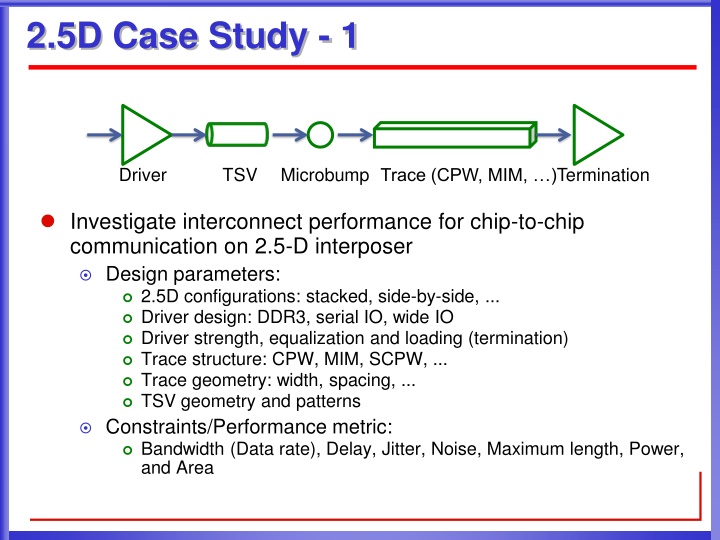
2.5D Case Study - 1 Driver TSV Microbump Trace (CPW, MIM, )Termination Investigate interconnect performance for chip-to-chip communication on 2.5-D interposer Design parameters: 2.5D configurations: stacked, side-by-side, ... Driver design: DDR3, serial IO, wide IO Driver strength, equalization and loading (termination) Trace structure: CPW, MIM, SCPW, ... Trace geometry: width, spacing, ... TSV geometry and patterns Constraints/Performance metric: Bandwidth (Data rate), Delay, Jitter, Noise, Maximum length, Power, and Area
2.5D Case Study - 1 Max length Max length @1GHz Driver 1 (DDR3) Driver 2 (serial IO) @3GHz Trace width Trace width Max data rate Power Stacked Driver 1 (DDR3) Driver 2 (wide IO) Side-by-side 10mm Trace width Trace length
2.5D Case Study - 1 Channel model TSV modeling (Done) Trace modeling (Siming, Wei) Microbump modeling (existing one?) Test-chip and measurement (Siming, Wei) Driver and termination model SPICE transistor-level model (from Cisco?) (Feng) Abstract model with ideal switch and RC networks (Feng) Performance estimation Matlab GUI with one-click automatic flow (Yubo) With SPICE simulation Extract jitter/noise/power from simulation results Without SPICE simulation Estimate jitter/noise/power directly from [RLGC]
Driver Models DDR3 Up to 4GHz Serial IO 10GHz, 16GHz Wide IO 250MHz Supported data rate # of IOs VDD Delay variation Jitter (timing window) SNR termination Matched 50ohm Matched 50ohm capacitive Power per bit Schematic
Channel Response channel Response p(t) for NRZ symbol s(t): step response = out data RX TX ( ) ( ) ( ) p t s t s t T Differential microstrip line Extract R, L, G, C Per-unit-length RLGC matrix Solve the multi-conductor distributed transmission line equations Here we have a two-conductor special case H(s): frequency response GS V(0) I(0) Y11 Y12 VO VS V(d) -I(d) Y21 Y22 ~ GL+sCL R, L, G, C, d = + + 1 ( ) ( G ( ) ) H s Y Y Y G 12 11 s s ~ = 1 ( ) Y Y Y G sC where 21 22 L L
Channel Response (contd) Frequency response compared to SPICE Pole-residue approximation = ( ) ( ) ( ) p t s t s t T SPICE
Pre-emphasis Filter Pre-emphasis filter Pre-filter the pulse with the inverse of the channel j = b W a + i j i j ai: input symbol bi: transmitter output Wj: filter coefficient channel out data RX TX FIR At receiver end i Pre-emphasis Filter RS = ( ) ( ) r t b p t iT i VNEAR VX2 VXM IW0 IW1 IWM
Jitter Model Timing jitter Time deviation of zero-crossing t t p = 0 ) ( t r = ) ( 1 received waveform r(t) p(t) 1 t v 0 , Vth 0 t T where 0 th = ( ) b p t iT v 1 i th i t0t1 Vth defines the zero level t0 is the crossing time without interference from other symbol or neighboring link t1 is the actual crossing time t1 t1 input pattern
Noise Model Amplitude noise amplitude variation at sampling time ts ( ) ( ) r t p t s s r(t) r(ts) p(ts) where p(t) ts input pattern
2.5D Case Study - 2 TSV array Microbump Bus (CPW, MIM, ) Termination Investigate interconnect crosstalk for chip-to-chip communication on 2.5-D interposer Design parameters: 2.5D configurations: stacked, side-by-side, ... Driver design: DDR3, serial IO, wide IO Driver strength, equalization and loading (termination) Trace structure: CPW, MIM, SCPW, ... Trace geometry: width, spacing, ... TSV geometry and patterns Constraints/Performance metric Crosstalk, Bandwidth (Data rate x pin count), Delay and delay variation, Jitter, Noise, Maximum length, Power, and Area Driver
2.5D Case Study - 2 Crosstalk Crosstalk From trace Driver 1 (DDR3) Driver 2 (serial IO) From TSV Data rate Data rate Max bandwidth Stacked Side-by-side 10mm Trace width
2.5D Case Study - 2 Channel model TSV array model (Done) Multi-trace bus model by Q3D (Nikos) Driver and termination model SPICE transistor-level model (from Cisco?) (Feng) Abstract model with ideal switch and RC networks (Feng) Performance estimation Crosstalk (Nikos) With SPICE simulation Extract crosstalk from simulation results Without SPICE simulation Estimate crosstalk directly from [RLGC] Matlab GUI with one-click automatic flow (Yubo)
2.5D Case Study - 3 Investigate interconnect noise for chip-to-chip communication on 2.5-D interposer Design parameters: 2.5D configurations: stacked, side-by-side, ... Driver design: DDR3, serial IO, wide IO Driver strength, equalization and loading (termination) Trace structure: CPW, MIM, SCPW, ... Trace geometry: width, spacing, ... TSV geometry and patterns Constraints/Performance metric SSN (Feng), ISI (Yubo), and Crosstalk (Nikos)
2.5D Case Study - 3 Channel model Driver and termination model (Feng) SPICE transistor-level model Abstract model with ideal switch and RC networks Noise transfer function (Feng) Performance estimation SSN (Feng) With SPICE simulation Extract SSN from simulation results Without SPICE simulation Estimate SSN directly from [RLGC]
Publication Opportunities 2.5D chip-to-chip communication case studies + test chip interconnect measurement results Channel synthesis/optimization for 2.5D chip-to-chip communication, considering TSV patterns, and/or Trace optimization and impedance control, For Different drivers, trace length, data rate, Satisfying constraints like delay, jitter, crosstalk, Crosstalk analysis and optimization for 2.5D TSV patterns and trace geometry CDMA-based crosstalk cancellation SSN for parallel bus and PDN design optimization SSN transfer function for different driver models PDN modeling Method to reduce SSN
Target Schedule ICCAD deadline (4/16) and End of quarter (3/23)
To-do List Feng DDR3, Serial-IO, Wide-IO driver model (abstract) DDR3, Serial-IO, Wide-IO driver model (transistor-level, if any) Supply noise to output driver transfer function On-chip PDN modeling Automatic matlab+SPICE function for SSN simulation Yubo Automatic matlab+SPICE function for single-link simulation Jitter/noise estimation from SPICE results Jitter/noise estimation given channel RLGC and driver models Nikos Interesting trace structures in 2.5D, especially considering crosstalk Extract RLGC for different trace structures (for parallel bus) Automatic matlab+SPICE function for crosstalk simulation Crosstalk analysis/estimation for traces given RLGC
To-do On-going Finished Feng Driver model and timing requirement for wide IO and serial IO Feng Complete the driver model table Driver model and timing requirement for DDR3 Yubo Show simulation results Expand RLGC->Y(s) to multiple- conductor Find H(s) with driver model and Y(s) Yubo Simulation platform for single-link Algorithms to extract jitter/noise from SPICE results Nikos Familiar with Q3D 3D modular and matrix reduction Determine what traces to test for crosstalk Nikos Build matlab/Q3D function for test traces RLGC->crosstalk
