Control Chip Functionality Overview in Particle Detection Systems
This detailed content discusses the functionality of the control chip in particle detection systems. It covers topics such as error monitoring, logic generation, input/output communication, and more. The control chip plays a crucial role in handling errors, generating actions based on severity, and ensuring smooth operation of the detection system. It also describes the monitoring of errors, handling of various signals, and the overall logic behind the control chip's operation in these systems.

Download Presentation

Please find below an Image/Link to download the presentation.
The content on the website is provided AS IS for your information and personal use only. It may not be sold, licensed, or shared on other websites without obtaining consent from the author.If you encounter any issues during the download, it is possible that the publisher has removed the file from their server.
You are allowed to download the files provided on this website for personal or commercial use, subject to the condition that they are used lawfully. All files are the property of their respective owners.
The content on the website is provided AS IS for your information and personal use only. It may not be sold, licensed, or shared on other websites without obtaining consent from the author.
E N D
Presentation Transcript
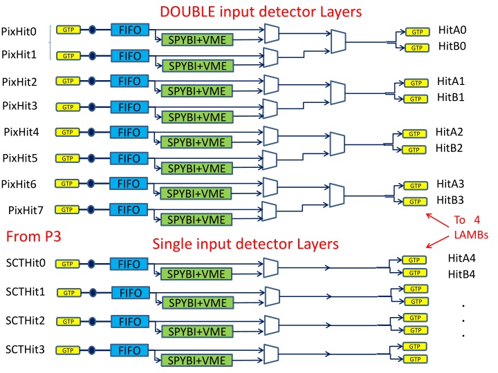
DOUBLE input detector Layers HitA0 HitB0 FIFO PixHit0 GTP GTP SPYBI+VME GTP PixHit1 FIFO GTP SPYBI+VME HitA1 HitB1 FIFO PixHit2 GTP GTP SPYBI+VME GTP PixHit3 FIFO GTP SPYBI+VME HitA2 HitB2 PixHit4 FIFO GTP GTP SPYBI+VME GTP PixHit5 FIFO GTP SPYBI+VME FIFO HitA3 HitB3 PixHit6 GTP GTP SPYBI+VME GTP FIFO PixHit7 GTP To 4 LAMBs SPYBI+VME From P3 Single input detector Layers HitA4 HitB4 GTP SCTHit0 FIFO GTP SPYBI+VME GTP GTP SCTHit1 FIFO GTP SPYBI+VME . . . GTP GTP SCTHit2 FIFO GTP SPYBI+VME GTP GTP SCTHit3 FIFO GTP SPYBI+VME GTP
AMBSLP HITA 4 Slinks 4 Slinks INPut Artix 12 S-links HITB 4 Slinks 16 Slinks 4 Slinks OUTput Artix
Control chip inputs/outputs (This is for AMBFTK to be updated) EE signals Signals to communicate Errors etc. Common to Input/output FPGAs VME signals Control Signals To VME chip
Control chip Logic: Generate INIT_event when: (a) EE is received by HIT, and ROAD chips (2 signals) Receive error (code & stream info) and generate an action (freeze or stopless-removal) comparing with Severity error For Freeze: check that the event involved in the error is totally processed and than generate the freeze to all AMBFTK FPGAs. Send Freeze upstream. Generate Operation Code to the LAMBs FSM?? Molto semplice: INIT_EVENT e quando riceve I 2 EE da HIT e ROAD, INIT_EVENT di nouvo. Init_event 1 2 2 EE words received
Errors to be monitored into the INPUT Chips Parity or CRC error for each link (8 pixel & 4 SCT) Parity (PA) or sum check should be monitored. Error detection should be registered in a 8 bit (or 4 bit word) FIFO Overflow each FIFO full flag should produce error if set. Again 8 (or 4) bit word. Invalid Input data (for example invalid HIT from ROD) ?? Lost Synchronism (event tags in different streams do not match) Again 8 (or 4) bit word Truncated output (for example too many hits in input) - Again 8 (or 4) bit word. We can communicate to Control Chip the error using: 4 bits to identify the kind of error + 8 (or 4) bits to say which is the faulty stream.
INPUT VME registers 1. Error register WR = clear; 8 (or 4) x 5 bits 2. For each FIFO: flag register (empty, HFull, Full) RO (3x 8 or 4) 3. For each FSM: state machine - RO 4. Output Status (Hold flags) RO (necessario? Esiste HFull) 5. For each Spy Buffer: Spy Buffer register: Pointer, OVFL flag, status(freeze/spy. WR=clear of Pointer & flag. Status is RO 6. chip firmware ID? (see Alberto slides) Firmware and date reg. 7. Input FiFos: R/W 8. Input Spy Buffers memories 9. Timing measurements: each chip has a counter. When Init_event is received it is started. When all the input EE event words are received it is stopped. All incoming words are written in the spy buffer with the counter content.