Understanding Semiconductors: Types, Properties, and Differences
Semiconductors bridge the gap between insulators and conductors, exhibiting varying levels of electrical conductivity based on temperature. This tutorial covers intrinsic semiconductors, differences between silicon and germanium, and the essential properties of semiconductors. Learn about the roles of carrier concentration, Fermi level, and optical transitions in semiconductors, along with practical applications and the mass action law.

Download Presentation

Please find below an Image/Link to download the presentation.
The content on the website is provided AS IS for your information and personal use only. It may not be sold, licensed, or shared on other websites without obtaining consent from the author. Download presentation by click this link. If you encounter any issues during the download, it is possible that the publisher has removed the file from their server.
E N D
Presentation Transcript
Solid state physics Solid state physics Lecture ( Lecture (3 3) ) semiconductors semiconductors Prof. Dr. Wisam J. Aziz
Contents -Introduction - Types of semiconductors -Carrier concentration and Fermi level - Mass Action Law - Carrier transport phenomena - Optical transition -Band to band transition -Applications of semiconductors
Introduction Introduction A semiconductor is a material with an electrical conductivity that is intermediate between that of an insulator and a conductor. A semiconductor behaves as an insulator at very low temperature, and has an appreciable electrical conductivity at room temperature although much lower conductivity than a conductor. It s called semiconductor because their ability to conduct electricity is small compared with the conductivity of metals Two general classifications of semiconductors are the elemental semiconductor materials ,found in group IV of periodic table , and compound semiconductor materials formed from the group III and V group .
The difference between conductors, semiconductors, and insulators
Intrinsic semiconductor Intrinsic semiconductor .
The difference between silicon and germanium Silicon - Silicon is denoted by Si and its atomic number is 14 - Semi-metallic - The atomic radius of silicon is less than the atomic radius of germanium - Conductivity of silicon Less than the conductivity of germanium - Silicon has no distribution Electrons in the d orbital Germanium - Germanium It is denoted by Ge and its atomic number is 32 - Semi-metallic - Be the atomic radius of germanium - Greater than the atomic radius of silicon - Germanium conductance Higher than the conductivity of silicon Most of the silicon specifications are ten times less expensive than the equivalent germanium specification, plus Silicon conductors are widely used due to Can be used at higher temperatures than conductors Germanium
Extrinsic Semiconductor Extrinsic Semiconductor Pure semiconductors have negligible conductivity at room temperature. To increase the conductivity of intrinsic semiconductor, some impurity is added. The resulting semiconductor is called impure or extrinsic semiconductor. 6 10 Impurities are added at the rate of ~ one atom per 10 to 10 semiconductor atoms. The purpose of adding impurity is to increase either the number of free electrons or holes in a semiconductor.
Extrinsic Semiconductor Extrinsic Semiconductor Two types of impurity atoms are added to the semiconductor Atoms containing 3 valance electrons (Trivalent impurity atoms) Atoms containing 5 valance electrons (Pentavalent impurity atoms) e.g. Al, B, In e.g. P, As , Bi N-type semiconductor P-type semiconductor Hole Free electron
N type semiconductor This figure shows an n- type silicon , where subsititutional phosphorous atom with 5 valance electrons has replaced a silicon atom , and negative charged electron is donated to the lattice in the conduction band. The phosphorous atom is called a donor . Si Si Si P Si Si Si Si Si
P type semiconductor This figure shows that when a boron atom with 3 valance electrons substitute for a silicon atom , a positive- charged hole is created in the valance band . And an additional electron will be accepted to form 4 covalent bonds around the boron. This is p type , and the boron is an accepter . Si Si Si Si Si B Si Si Si
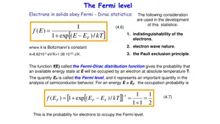
Carrier concentration and Fermi level Carrier concentration and Fermi level We first consider the intrinsic case without impurities added to the semiconductor. The number of electrons (occupied conduction- band levels) is given by the total number of states N(E) multiplied by the occupancy F(E), integrated over the conduction band: The no. of electron is given by : c E = ( ) ( ) n f E N E dE 1 0 where where N(E) the energy range the energy range dE N(E)dE dE : : is the density of states (cm is the density of states (cm- -3 3) in dE ) in F(E) : fermi F(E) : fermi - - dirac distribution function dirac distribution function
Intrinsic semiconductors Where : where Nvis the effective density of states in the valence band Nc : the effective density of states in the condition band Ec : energy of states in condition band Ev : energy of states in valance band K : boltazman constant T : temperature the concentration of electrons in the conduction band is the concentration of holes in the valance band is Extrinsic semiconductors n-type p-type = = exp ( / ) p n E E kT exp ( / ) n n E E kT 0 i i F 0 i F i
Fermi energy Fermi energy or the Fermi level in solid and matter physics The capacitor represents the highest energy level an electron occupies at a degree Absolute zero. At zero kelvin (absolute zero), no The electrons gain any heat energy that helps them move. it begins by filling in the lowest energy levels in "clusters of atoms" first then the upper, the higher, forming a sea of electrons called a sea Fermi. The surface of this sea represents "Fermi energy".
Mass Action Law Mass Action Law Addition of n-type impurities decreases the number of holes below a level. Similarly, the addition of p-type impurities decreases the number of electrons below a level. It has been experimentally found that Under thermal equilibrium for any semiconductor, the product of no. of holes and the no. of electrons is constant and independent of amount of doping. This relation is known as mass action law = 2 . n p in where n = electron concentration, p = hole concentration and ni = intrinsic concentration
Carrier Carrier transport phenomena transport phenomena 1- Drift and Mobility . At low electric fields the drift velocity is proportional to the electric field strength ? and the proportionality constant defined as mobility ?. Since the mobility is controlled by scattering it can be also related to the mean free time ?m .or mean free bath by The last result use the relationship Where : is the thermal velocity given by
For multiple scattering mechanics , the effective mean free time is derived from the individual mean free times of scattering events by As the impurity concentration increases ( at room temp. ) the mobility decrease also for larger , mobility decreases ; thus for given impurity concentration the electron mobilites for these semiconductor are larger than the hole mobilites For lower impurity concentration the mobility is limited by phonon scattering and it decreases with temp .
Resistivity For semiconductors with both electron and holes as carriers, the drift current under applied field is given by : Where ? is the conductance Where ? is the resistivity , if n >> p
Recombination, Generation, and Carrier Lifetimes Whenever the thermal-equilibrium condition of a semiconductor system is disturbed processes exist to restore the system to equilibrium. These processes are recombination when and thermal generation when .
Figure below illustrates the band-to-band electron-hole recombination. The energy of an electron in transition from the conduction band to the valence band is conserved by emission of a photon ( radiative process) or by transfer of the energy to another free electron or hole (Auger process). The former process is the inverse of direct optical absorption, and the latter is the inverse of impact ionization. Band-to-band transitions are more probable for direct-band gap semiconductors which are more common among 111-V compounds. For this type of transition, the recombination rate is proportional to the product of electron and hole concentrations, given by The term called the recombination coefficient .
Recombination processes (the reverse are generation processes). (a) Band-to-band recombination. Energy is exchanged to a radiative or Auger process. (b) (b) Recombination through single-level traps (non radiative).
Optical transitions (a) allowed (b) forbidden direct transitions (c) indirect transition involving phonon emission (upper arrow) and phonon absorption (lower arrow).
Band to band transition There are two transition (allowed and forbidden ) . Direct transition : Allowed direct transition can occur in all K values and =1/2 . Forbidden direct transition can only occur at k 0 and = 3/2 . Indirect transition : Phonons are involved in order to conserve momentum . In these transition , phonons (with energy Ep) are either absorbed or emitted, and the absorption coefficient is modified to = 2 & 3 for allowed and forbidden indirect transition , respectively .
Applications of semiconductors A-In electronic devices 1-Computers, television and mobile devices 2-High brightness LEDs. 3-Imaging array sensors: Digital cameras. 4-Diode lasers. 5-Optical storage. 6-Robotics. 7-Medical Electronics. 8-Industrial Electronics. 9-Telecommunications. 10-Wireless Communication. 11-Global Positioning By Satellite (GPS). 12-Memories. B-in solar cells C-In telecommunications D- Technical field