Understanding Fermi-Dirac Statistics in Solids
Electrons in solids obey Fermi-Dirac statistics, governed by the Fermi-Dirac distribution function. This function describes the probability of electron occupation in available energy states, with the Fermi level representing a crucial parameter in analyzing semiconductor behavior. At different temperatures, the function dictates the probabilities of states being occupied or empty relative to the Fermi level, providing insights into electron and hole concentrations in semiconductors. The distribution function enables the calculation of electron and hole concentrations in equilibrium by considering the density of states in conduction and valence bands alongside the probability of occupancy.
Download Presentation

Please find below an Image/Link to download the presentation.
The content on the website is provided AS IS for your information and personal use only. It may not be sold, licensed, or shared on other websites without obtaining consent from the author. Download presentation by click this link. If you encounter any issues during the download, it is possible that the publisher has removed the file from their server.
E N D
Presentation Transcript
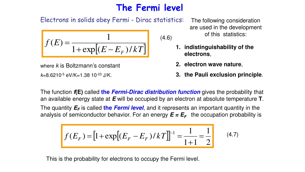
The Fermi level Electrons in solids obey Fermi - Dirac statistics: The following consideration are used in the development of this statistics: 1 (4.6) = ( ) f E + 1. indistinguishability of the electrons, 1 exp ( F/ ) E E kT 2. electron wave nature, where k is Boltzmann s constant 3. the Pauli exclusion principle. k=8.62 10-5 eV/K=1.38 10-23 J/K. The function f(E) called the Fermi-Dirac distribution function gives the probability that an available energy state at E will be occupied by an electron at absolute temperature T. The quantity EF is called the Fermi level, and it represents an important quantity in the analysis of semiconductor behavior. For an energy E = EF the occupation probability is 1 + 1 1 1 = + = = (4.7) ( ) exp ( / ) F f E E E kT F F 1 1 2 This is the probability for electrons to occupy the Fermi level.
The Fermi Dirac distribution function At T=0K f(E) has rectangular shape the denominator of the exponent is 1/(1+0)=1 when (E<Ef), exp. negative 1/(1+ )-0 when (E>Ef), exp. positive At 0 every available energy state up to EF is filled with electrons, and all states above EF are empty. At temperatures higher than 0 K, some probability f(E) exists for states above the Fermi level to be filled with electrons and there is a corresponding probability [1 - f(E)] that states below EF are empty. The Fermi function is symmetrical about EF for all temperatures. The probability exists for The Fermi Dirac distribution function for different temperatures state E above EF is filled f(EF+ E) state E below EF is filled [1- f(EF - E)] The symmetry of the distribution of empty and filled states about EF makes the Fermi level a natural reference point in calculations of electron and hole concentrations in semiconductors. In applying the Fermi-Dirac distribution to semiconductors, we must recall that f(E) is the probability of occupancy of an available state at E. Thus if there is no available state at E (e.g., in the band gap of a semiconductor), there is no possibility of finding an electron there.
Relation between f(E) and the band structure Electron probability tail f(E) Hole probability tail [1-f(E)] In intrinsic material the Fermi level EF must lie at the middle of the band gap. In n-type material the distribution function f(E) must lie above its intrinsic position on the energy scale. The energy difference (Ec EF) gives a measure of n. For p-type material the Fermi level lies near the valence band such that the [1-f(E)] tail below Ev is larger than the f(E) tail above Ec. The value of (EF Ev) indicates how strongly p-type the material is. The distribution function has values within the band gap between E and Ec, but there are no energy states available, and no electron occupancy results from f(E) in this range.
Electron and Hole Concentrations at Equilibrium The Fermi distribution function can be used to calculate the concentrations of electrons and holes in a semiconductor if the densities of available states in the valence and conduction bands are known. The concentration of electrons in the conduction band is c E where N(E)dE is the density of states (cm-3) in the energy range dE. The subscript 0 used for the electron and hole concentration symbols (n0, p0) indicates equilibrium conditions. = ( ) ( ) n f E N E dE (4.8) 0 The number of electrons per unit volume in the energy range dE is the product of the density of states and the probability of occupancy f(E). Thus the total electron concentration is the integral over the entire conduction band. The function N(E) can be calculated by using quantum mechanics and the Pauli exclusion principle. N(E) is proportional to E1/2, so the density of states in the conduction band increases with electron energy. On the other hand, the Fermi function becomes extremely small for large energies. The result is that the product f(E)N(E) decreases rapidly above Ec, and very few electrons occupy energy states far above the conduction band edge. Similarly, the probability of finding an empty state (hole) in the valence band [1 - f(E)] decreases rapidly below Ev, and most holes occupy states near the top of the valence band.
Band diagram, density of states, Fermi-Dirac distribution, and the carrier concentrations at thermal equilibrium Intrinsic semiconductor n-type semiconductor p-type semiconductor
The conduction band electron concentration is simply the effective density of states at Ec times the probability of occupancy at Ec: ( 0 c f N n = ) E (4-9) c In this expression we assume the Fermi level EF lies at least several kT below the conduction band. Then the exponential term is large compared with unity, and the Fermi function f(Ec) can be simplified as 1 (4-10) = ( ) exp ( / ) f E E E kT c c F + 1 exp ( / ) E E kT c F Since kT at room temperature is only 0.026 eV, this is generally a good approximation. For this condition the concentration of electrons in the conduction band is = exp ( / ) n N E E kT (4-11) 0 c c F It can be shown that the effective density of states Nc is * n 2 m kT (4-12) = / 3 ) 2 ( 2 N c 2 h Values of Nc can be tabulated as a function of temperature. As Eq. (4-11) indicates, the electron concentration increases as EF moves closer to the conduction band. By similar arguments, the concentration of holes in the valence band is = 1 [ v ( )] p N f E (4-13) 0 v where Nvis the effective density of states in the valence band.
The probability of finding an empty state at Ev, is 1 = 1 ( ) 1 exp ( / ) f E E E kT (4-14) v F v + 1 exp ( / ) E E kT v F for EF larger than Ev by several kT. From these equations, the concentration of holes in the valence band is = exp ( / ) p N E E kT (4-15) 0 v F v The effective density of states in the valence band reduced to the band edge is * p 2 m kT = / 3 ) 2 (4-16) ( 2 N v 2 h Eq. (4-15) predicts that the hole concentration increases as EF moves closer to the valence band. The electron and hole concentrations predicted by Eqs. (4-11) and (4-15) are valid whether the material is intrinsic or doped, provided thermal equilibrium is maintained. Thus for intrinsic material, EF lies at some intrinsic level Ei near the middle of the band gap, and the intrinsic electron and hole concentrations are (4-17) = exp ( / ) = p N E E kT exp ( / ) n N E E kT , i v i v i c c i
The product of n0 and p0 at equilibrium is a constant for a particular material and temperature, even if the doping is varied: = ) = ( exp ( / ) F kT / ) )( exp ( / ) v n p N E E kT N E E kT (4-18a) 0 0 c c v F = = exp ( exp / N N E E N N E kT c v c v c v g = ) = ( exp ( / ) i )( exp ( / ) v n p N E E kT N E E kT (4-18b) i i c c v i = exp / N N E kT c v g In Eqns. (4-18a) and (4-18b) Eg = Ec Ev. The intrinsic electron and hole concentrations are equal (since the carriers are created in pairs), ni= pi ; thus the intrinsic concentration is = (4-19) exp( / 2 ) n N N E kT i c v g The constant product of electron and hole concentrations in Eq. (4-18) can be written conveniently as = 2 n p in (4-20) 0 0 This is an important relation, and we shall use it extensively in later calculations. The intrinsic concentration for Si at room temperature is approximately ni = 1.5 x 1010cm-3.
Comparing Eqs. (4-17) and (4-19), we note that the intrinsic level Ei is the middle of the band gap (Ec - Ei= Eg/2), if the effective densities of states Ncand Nv are equal. There is usually some difference in effective mass for electrons and holes (e.g. for Si mn*=0.26m0, mn*=0.39m0),however, and, therefore, Nc and N are slightly different as Eqs. (4-12) and (4-16) indicate. Another convenient way of writing Eqs. (4-11) and (4-15) is = exp ( / ) n n E E kT (4-21) 0 i F i = exp ( / ) p n E E kT (4-22) 0 i i F obtained by the application of Eq. (4-17). This form of the equations indicates directly that the electron concentration is ni, when EF is at the intrinsic level Ei, and that n0 increases exponentially as the Fermi level moves away from Ei toward the conduction band. Similarly, the hole concentration p0 varies from ni, to larger values as EF moves from Ei toward the valence band. Since these equations reveal the qualitative features of carrier concentration so directly, they are particularly convenient to remember.
