Understanding Noise in RF Integrated Circuits: Thermal and 1/f Noise

Noise, an unwanted input, limits a system's ability to process weak signals. Sources of noise include random noise in resistors and transistors, mixer noise, undesired cross-coupling noise, and power supply noise. Thermal noise, caused by thermal agitation of charge carriers, is also known as Johnson-Nyquist noise. 1/f noise, or flicker noise, is an irreducible form of noise with a power spectrum that decreases by 10dB per decade of frequency. Flicker noise in electrical and electronic devices is primarily observed when electric current flows, especially in semiconductors due to traps trapping carriers temporarily. The corner frequency, Fc, is a crucial parameter for 1/f noise, marking where the power spectral density equals the white noise level.

Download Presentation

Please find below an Image/Link to download the presentation.
The content on the website is provided AS IS for your information and personal use only. It may not be sold, licensed, or shared on other websites without obtaining consent from the author. Download presentation by click this link. If you encounter any issues during the download, it is possible that the publisher has removed the file from their server.
E N D
Presentation Transcript
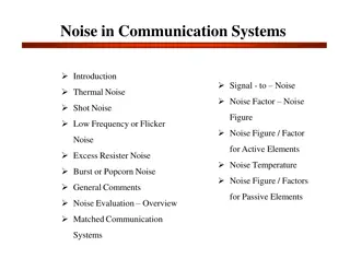
RF INTEGRATED CIRCUITS UNIT-III
RFIC UNIT-III Noise Any unwanted input Limits systems ability to process weak signals Sources: 1.Random noise in resistors and transistors 2.Mixer noise 3.Undesired cross-coupling noise 4.Power supply noise Dynamic range capability of detecting weak signals in presence of large-amplitude signals
3 1. Thermal noise Thermal noise is observed in any system having thermal losses and is caused by thermal agitation of charge carriers. Thermal noise is also called Johnson-Nyquist noise. (Johnson, Nyquist: 1928, Schottky: 1918). An example of thermal noise can be thermal noise in resistors.
7 5.2.3. 1/f noise Thermal noise and shot noise are irreducible (ever present) forms of noise. They define the minimum noise level or the noise floor . Many devices generate additional or excess noise. The most general type of excess noise is 1/f or flicker noise. This noise has approximately 1/f power spectrum (equal power per decade of frequency) and is sometimes also called pink noise. 1/f noise is usually related to the fluctuations of the device properties caused, for example, by electric current in resistors and semiconductor devices. Curiously enough, 1/f noise is present in nature in unexpected places, e.g., the speed of ocean currents, the flow of traffic on an expressway, the loudness of a piece of classical music versus time, and the flow of sand in an hourglass. No unifying principle has been found for all the 1/f noise sources. Reference: [3]
8 In electrical and electronic devices, flicker noise occurs only when electric current is flowing. In semiconductors, flicker noise usually arises due to traps, where the carriers that would normally constitute dc current flow are held for some time and then released. Although bipolar, JFET, and MOSFET transistors have flicker noise, it is a significant noise source in MOS transistors, whereas it can often be ignored in bipolar transistors (and some modern JFETs). References: [4] and [5]
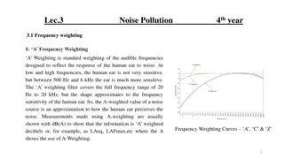
9 An important parameter of 1/f noise is its corner frequency, fc, where the power spectral density equals the white noise level. A typical value of ff is 100 Hz to 1 kHz (MOSFET: 100 kHz). in (f), dB 10dB/decade Pink noise White noise f,decades ff
Noise (contd.) noisiness of the signal measure = signal-to-noise ratio (frequency dependant) ( ) S f average signal power = = SNR ( ) N f average noise power Random noise External Atmospheric Interstellar Receiver internal Thermal Flicker noise (low frequency) Shot noise
Noise factor IEEE Standards: The noise factor, at a specified input frequency, is defined as the ratio of (1) the total noise power per unit bandwidth available at the output port when noise temperature of the input termination is standard (290 K) to (2) that portion of (1) engendered at the input frequency by the input termination. available output noise power = F available output noise due to source
Noise factor (cont.) + ( ( ) ) N G f N S S N N ( i a i i o a ) = = = + 1 F N S N S G f N i o i o i It is a measure of the degradation of SNR due to the noise added - Implies that SNR gets worse as we process the signal Spot noise factor The answer is the bandwidth SNR i = 1 F SNR o N a =1 + F kT
Noise factor (cont.) Quantitative measure of receiver performance wrt noise for a given bandwidth Noise figure Typically 8-10 db for modern receivers Multistage (cascaded) system 1 + + = G NF = 10 log( ) F G 1 1 1 G F F F 2 3 n + + ... F F G G G 1 1 2 1 2 1 n
Noise Figure Definition SNR S N = = in in in NF SNR S N out out out As a function of device + N G N = device source NF G N source G: Power gain of the device
NF of Cascaded Stages Sin/Nin Sout/Nout G1, N1, NF1 Gi, Ni, NFi GK, NK, NFK 1 1 1 NF NF NF = + + + + 3 G 1 1 2 K ...G NF NF ... 1 G G G G 1 1 2 1 2 1 K Overall NF dominated by NF1 [1] F. Friis, Noise Figure of Radio Receivers, Proc. IRE, Vol. 32, pp.419-422, July 1944.
Simple Model of Noise in MOSFET k = 2 ( ) V f Flicker noise Dominant at low frequency Thermal noise : empirical constant 2/3 for long channel much larger for short channel PMOS has less thermal noise g WLC f Vg ox Id = 2 ( ) 4 I f kT g d m Vi Input-inferred noise k = + 2 ( ) 4 V f kT i g WLC f m ox
Noise Approximation Noise spectral density 1/f noise Thermal noise dominant Thermal noise Frequency Band of interest
Low-Noise Amplifier First gain stage in receiver Amplify weak signal Significant impact on noise performance Dominate input-referred noise of front end 1 NF subsequent G = + NF NF frontend LNA LNA Impedance matching Efficient power transfer Better noise performance Stable circuit
RF Receiver Antenna BPF1 LNA BPF2 Mixer BPF3 IF Amp Demodulator RF front end LO
LNA Design Consideration Noise performance Power transfer Impedance matching Power consumption Bandwidth Stability Linearity
S-Parameters Parameters for two-port system analysis Suitable for distributive elements Inputs and outputs expressed in powers Transmission coefficients Reflection coefficients
S-Parameters S11 input reflection coefficient with the output matched b = 1 S 11 a 1 = 2 0 a b S21 forward transmission gain or loss = 2 S 21 a 1 = 2 0 a S12 reverse transmission or isolation b = 1 S 12 a 2 S22 output reflection coefficient with the input matched = 1 0 a b = 2 S 22 a 2 = 1 0 a
S-Parameters I1 I2 Z1 S Z2 Vs1 V1 V2 Vs2 * 1 * 2 Re( ) V I Z V I Z Z = = 1 1 2 2 1 S S 11 21 + + Re( ) V I Z V I Z Z 1 1 1 1 1 1 2 = 0 V = 0 V 2 s 2 s * 1 * 2 Re( ) V I Z Z V I Z = = 1 1 2 2 2 S S 12 22 + + Re( ) V I Z Z V I Z 2 2 2 1 2 2 2 = 0 V = 0 V 1 s 1 s
A First LNA Example io Assume No flicker noise ro = infinity Cgd = 0 Reasonable for appropriate bandwidth Effective transconductance i G = = Rs Vs Rs 4kTRs g Z o m in meff Vs Vgs + V R Z 4kT gm gmVgs s s in
Power Gain Voltage input Current output 2 * o i i g Z = = = 2 | | o m in G G meff + * V V R Z s s s in 2 2 1 ( ) g j C g m gs = = m R + + 1 ( ) 1 R j C j C s gs s gs 2 2 m R 1 R g = T + 2 2 1 ( ) C s gs s
Series-Shunt Feedback RF Broadband matching RL Rs + + + ( )( 1 ) R R + g R sR C F L R m ( a a + gs R = R in + + + 1 ( ) C ) g R s R R Vs m L a a F + L gs Ra + 1 ( + )( ) g R R R + = R m + a F s out 1 ( )( + ) g sC R R m gs s a + ( ) sC R R + R R R R gs + a F s F R a s + iout Rs RF + 1 ( )( ) g sC R m gs s a RL Could be noisy Cgs Vgs gmVgs Vs Ra
Cascode Isolation to improve S12 @ high frequency Small range at Vd1 Reduced feedback effect of Cgd Improve noise performance LL Vo Vbias M2 Vd1 Lg Rs M1 Vs Ls
MIXERS Frequency translation device Convert RF frequency to a lower IF or base band for easy signal processing in receivers Convert base band signal or IF frequency to a higher IF or RF frequency for efficient transmission in transmitters
An ideal nonlinearity mixer t A t x 1 cos ) ( = = ( ) cos If x(t)y(t) x(t) y t B t 2 y(t) Then the output is AB 2 AB 2 = + + cos cos cos( ) cos( ) A t B t t t 1 2 1 2 1 2 down convert up convert
Suarelaw mosfet Voltage temperature equivalent
Simple Switching Mixer (Single Balanced Mixer) The transistor M1 converts the RF voltage signal to the current signal. Transistors M2 and M3 commute the current between the two branches. RL RL Vout VLO +VLO M3 M2 + I I DC RF M1 VRF
Double Balanced Mixer RL RL VOUT +VLO VLO +VLO M3 M3 M2 M2 + I I I I DC RF DC RF +VRF VRF Strong LO-IF feed suppressed by double balanced mixer. All the even harmonics cancelled. All the odd harmonics doubled (including the signal).
In sample(track) mode: M1 through M5 turned on while M6 and M7 are placed in the OFF state Devices M3,M4 and M5 put a voltage equal to the Common Mode Voltage levels VCM of the sampling capacitors while Input switches M1,and M2 connect the capacitors to the RF Input signal. Because M6 and M7 are open the op-amp is irrelevant in this tracking mode the tracking bandwidth is simply set by the RC time constant R..is Total Switching Resistance and C ..is Sampling capacitance In hold mode: In hold mode all switches are reversed, so that the conducting Transistors are M6 and M7 are the two feedback devices. In this mode the circuit degenerates to a pair of charged capacitors feeding back around the op-amp Properly designed track-and-hold circuit works as sub- sampling mixer. The sampling clock s jitter must be very small Subsampling mixers can exhibit large noise figures. Subsampling can exhibit mixers high linearity
Properly designed track-and-hold circuit works as sub-sampling mixer. The sampling clock s jitter must be very small Noise folding leads to large mixer noise figure. High linearity
Gilbert Mixer Use a differential pair to achieve the transconductor implementation This is the preferred mixer implementation for most radio systems!


")

")
")


")


 mode: M1 through M5 turned on while M6 and")