Efficient Class B Amplifier Operation and Power Calculation
Class B amplifiers offer greater efficiency compared to single transistor Class A operation. This article covers the push-pull operation of Class B transistors, input DC power calculations, connecting push-pull amplifiers to loads, output AC power measurement, efficiency calculation, and power dissipation by output transistors. Understanding these concepts helps optimize circuit performance and power delivery.

Download Presentation

Please find below an Image/Link to download the presentation.
The content on the website is provided AS IS for your information and personal use only. It may not be sold, licensed, or shared on other websites without obtaining consent from the author. Download presentation by click this link. If you encounter any issues during the download, it is possible that the publisher has removed the file from their server.
E N D
Presentation Transcript
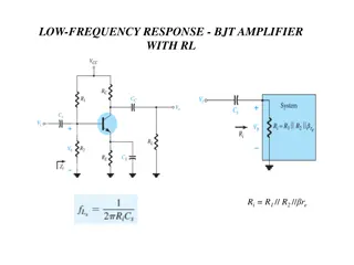
CLASS B AMPLIFIER OPERATION Page 693 -703
the class B operation of these transistors provides greater efficiency than was possible using a single transistor in class A operation. Block representation of push-pull operation.
Input (DC) Power where Idc is the average or dc current drawn from the power supplies.
Figure 16.13 Connection of push-pull amplifier to load: (a) using two voltage supplies; (b) using one voltage supply.
the current drawn from a single power supply has the form of a full-wave rectified signal, while that drawn from two power supplies has the form of a half wave rectified signal from each supply the average current drawn is: where I(p) is the peak value of the output current waveform.
Output (AC) Power If one is using an oscilloscope, the peak, or peak-to-peak, output voltage measured can be used: The larger the rms or peak output voltage, the larger the power delivered to the load.
Efficiency The efficiency of the class B amplifier can be calculated using the basic equation
the larger the peak voltage, the higher the circuit efficiency, up to a maximum value when VL(p) = VCC, this maximum efficiency then being Power Dissipated by output Transistor The power dissipated (as heat) by the output power transistors is the difference between the input power delivered by the supplies and the output power delivered to the load.
where P2Qis the power dissipated by the two output power transistors. The dissipated power handled by each transistor is then
Maximum Power Considerations For class B operation, the maximum output power is delivered to the load when VL(p) = VCC:
For class B operation, the maximum power dissipated by the output transistors does not occur at the maximum power input or output condition. The maximum power dissipated by the two output transistors occurs when the output voltage across the load is
The maximum efficiency of a class B amplifier can also be expressed as follows:
CLASS B AMPLIFIER CIRCUITS Figure 16.14 shows different ways to obtain phase-inverted signals from a single input signal. Figure 16.14a shows a center-tapped transformer to provide opposite phase signals. If the transformer is exactly center- tapped, the two signals are exactly opposite in phase and of the same magnitude.
Fig. 16.14b uses a BJT stage with in-phase output from the emitter and opposite phase output from the collector. If the gain is made nearly 1 for each output, the same magnitude results.
Probably most common would be using op- amp stages, one to provide an inverting gain of unity and the other a noninverting gain of unity, to provide two outputs of the same magnitude but of opposite phase
Transformer-Coupled PushPull Circuits
During a complete cycle of the input, a complete cycle of output signal is developed across the load. One disadvantage of the circuit is the need for two separate voltage supplies. Another, less obvious complementary circuit is shown in the resulting crossover distortion in the output signal (see Fig. 16.16d). Crossover distortion refers to the fact that during the signal crossover from positive to negative (or vice versa) there is some nonlinearity in the output signal. This results from the fact that the circuit does not provide exact switching of one transistor off and the other on at the zero-voltage condition. Both transistors may be partially off disadvantage with the
so that the output voltage does not follow the input around the zero-voltage condition. Biasing the transistors in class AB improves this operation by biasing both transistors to be on for more than half a cycle.
A more practical version of a push-pull circuit using complementary transistors is shown in Fig. 16.17. Note that the load is driven as the output of an emitter follower so that the load resistance of the load is matched by the low output resistance of the driving source. The circuit uses complementary Darlington- connected transistors to provide higher output current and lower output resistance.
Quasi-Complementary PushPull Amplifier In practical power amplifier circuits, it is preferable to use npn transistors for both high- current-output devices. Since the push-pull connection requires complementary devices, a pnp high-power transistor must be used. A practical means of obtaining complementary operation while using the same, matched npn transistors for the output is provided by a quasi- complementary circuit, as shown in Fig. 16.18.
Resistor R2 can be adjusted to minimize crossover distortion by adjusting the dc bias condition.


 Power")


 Power")