Microelectronic System Design by P. Bruschi - Overview of Cascode Current Mirrors and Wide Swing Configurations

Explore the detailed design of microelectronic systems by P. Bruschi, focusing on cascode current mirrors and wide swing configurations. The content includes various images illustrating classic and non-optimal topologies, parameters, and voltage shifters for MOSFET mirrors. Learn about high precision designs for wide swing cascode mirrors and the neglect of body effects in mirror configuration.

Download Presentation

Please find below an Image/Link to download the presentation.
The content on the website is provided AS IS for your information and personal use only. It may not be sold, licensed, or shared on other websites without obtaining consent from the author. Download presentation by click this link. If you encounter any issues during the download, it is possible that the publisher has removed the file from their server.
E N D
Presentation Transcript
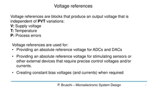
( ) = + + 1 R r r g r 1 2 2 1 out d d m d P. Bruschi Microelectronic System Design 1
CMOS cascode current mirror (classic topology) VB1=VB2=VB3=VB4=Vss (lowest supply rail) VBS2=VBS1 VBS3 generally BS4 P. Bruschi Microelectronic System Design 4
CMOS cascode current mirror (classic topology) P. Bruschi Microelectronic System Design 5
CMOS cascode current mirror (classic topology) Parameters ( ) ( ) = + = + + + V V = V V V V V V V 1 3 1 3 in GS V GS V + t t GS t GS t 1 3 = + V V DSAT V 2 4 2 4 MIN DS DSAT GS 1 ( ) ( ) ( ) = + + + = + 1 1 1 R r r g r r g r g r 4 2 4 4 2 4 4 2 4 2 out d d m d d m d m d I 4 D ( ) + 1 1 V out out R I g r 4 4 2 th m d P. Bruschi Microelectronic System Design 6
Cascode current mirror: non-optimal VMIN P. Bruschi Microelectronic System Design 7
Wide swing cascode mirror: 6 MOSFET mirror Voltage shifter = k 2 M 1 = + V V V V V 2 1 3 6 4 DS GS GS GS GS ( + ) ( ) ( ) ( ) = + + V V V V V V V V V 2 DS GS V t GS t GS t GS t 1 3 6 4 V V V 1 3 6 4 t t t t P. Bruschi Microelectronic System Design 8
Wide swing cascode mirror: 6 MOSFET mirror (neglecting the body effect) + 0 V V V V 1 3 6 4 t t t t ( ) ( ) ( ) ( ) = + V V V V V V V V V 2 DS GS t GS t GS t GS t 1 3 6 4 In strong inversion: 2 2 2 2 I I I I = + 3 6 D D V 1 4 D D 2 DS 1 3 6 4 Choices: ID5=ID1 (=ID6) 6= 1 4=kM 1 3= 1/4 2 42 2 2 I I I k I k = + V 1 1 1 1 D D D M D 2 DS 1 1 1 1 M 2 I ( ) = = = 2 V V V DSAT V 1 D 2 1 2 DS GS t 1 P. Bruschi Microelectronic System Design 9
High precision wide swing cascode mirror = k 2 M 1 = = V V V V V V 1 3 DS k GS 2 4 DS k GS = = V V V V 2 1 3 4 DS DS GS GS = 4 2 = V V 3 1 1 IN GS P. Bruschi Microelectronic System Design 10
= V V V ( V 2 4 DS K GS ) = ( V V V ) V V 2 4 DS K GS t t 4 + = 1 V = V + m 4 V 0 4 4 m t t SB ( ) ( ) 1 1 m V V 0 4 4 4 4 t S B = V V 4 2 S DS ( m + ( ) ) ) + 1 1 V V m V V 4 0 4 2 4 4 t t DS ) V B ) ( ( ( = 1 1 V V V V V m m V 2 0 4 2 4 4 DS k GS t t DS B 4 ( ) ( ) + + 1 V m V V V V m V 4 2 0 4 4 k DS GS t t B 4 P. Bruschi Microelectronic System Design 11
Bias of a wide-swing cascode structure ( ) ( ) = + + ) 1 V V m V V V V m V 5 4 V 2 + 0 4 4 k GS ( DS ) 5 GS + t t B 4 1 ( V V V m V 5 0 5 5 GS GS t t BS ( ) ( ) + V V mV V V 2 4 GS t DS GS t 5 4 P. Bruschi Microelectronic System Design 12
To reach maximum swing: V DSAT V 2 2 DS In strong inversion ( ) = V DSAT V V V 2 2 DS GS t 2 ( ) ( ) ( ) + V V m V V V V 4 4 GS t GS t GS t 5 2 4 = = V V V ( V V V V 3 1 3 4 D GS k t k t ) + V V V 1 2 GS DS GS t 4 P. Bruschi Microelectronic System Design 13
P-version of the wide swing high precision cascode mirror Very important rule: Voltage Vk must be invariant against Vdd variations when measured using Ref as the reference voltage. (i.e. Vk should be referred to node Ref.) The circuit shown in the picture satisfies this requirement. P. Bruschi Microelectronic System Design 14


")
")
")