Understanding Band-Gap Voltage References in Microelectronic Systems
Voltage references provide stable output voltages unaffected by variations in supply voltage, temperature, and process errors. This summary delves into the principles of band-gap voltage references and their crucial role in creating precise control voltages for ADCs, DACs, and various other applications in microelectronic systems.

Download Presentation

Please find below an Image/Link to download the presentation.
The content on the website is provided AS IS for your information and personal use only. It may not be sold, licensed, or shared on other websites without obtaining consent from the author. Download presentation by click this link. If you encounter any issues during the download, it is possible that the publisher has removed the file from their server.
E N D
Presentation Transcript
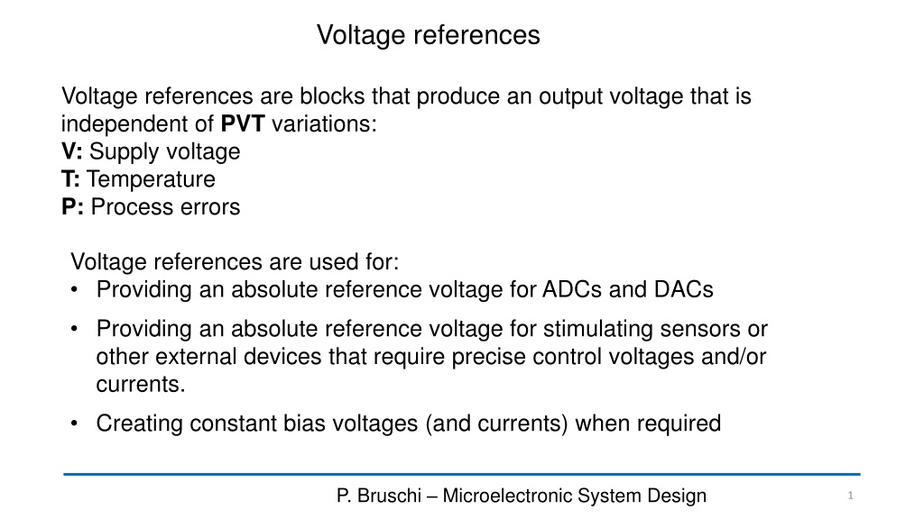
Voltage references Voltage references are blocks that produce an output voltage that is independent of PVT variations: V: Supply voltage T: Temperature P: Process errors Voltage references are used for: Providing an absolute reference voltage for ADCs and DACs Providing an absolute reference voltage for stimulating sensors or other external devices that require precise control voltages and/or currents. Creating constant bias voltages (and currents) when required P. Bruschi Microelectronic System Design 1
Possible reference voltage sources Zener Diodes Problems: Require additional process steps, but only a small number of components are required for each chip (not convenient) Available voltages are > 3 V Temperature stability is poor for VZ 5-6 V The reference voltage generated by a Zener diode is noisy (very wide band noise) In present days, zener diodes are available only in high voltage processes and are used more for protection than for voltage references Band-gap circuits solution P. Bruschi Microelectronic System Design 2
Band-gap voltage reference: principle of operation We start with a DIODE (BJT) biased with a current IC VBG PTAT VPTAT CTAT CTAT: Complementary To Absolute Temperature = + V V bV BG BE T PTAT: Proportional To Absolute Temperature dV dT @- 2 mV/K ..... - 3 mV/K BE P. Bruschi Microelectronic System Design 3
Band-gap voltage reference: determination of parameter b and estimate of the output voltage dV dT We have to determine the value of b, for which: = + V V bV = 0 BG BG BE T dV dT dV dT dV dT dV dT dV dT Good news! This voltage is compatible with low-supply voltage circuits - BE = + = 0 BG b BE T = b T dV dT k q - 5 8.56 10 / V K T = @ V (290K) T V BE Example: dV dT @- 2 mV/K BE 23 b @ = 1.225 V 0.65 0.025 23 V @ + BG P. Bruschi Microelectronic System Design 4
Band-Gap voltage reference: theory E kT 0 g constant 2 3 in T e I 2 i qA n D = ln V V C = F n D 2 i = E Q n I BE T n I S kT q = D S B n n E kT E V V q V V 0 G 0 0 g g = = 0 G = = 4 SI BT e T T q k T T n 1.5 VG0 constant constant IC= It is not necessary that ICis temperature-independent integrated circuits" 4th edition, 2001 J.Wiley & Sons GT 1 B = E GT ( ) ( ) ( ) ln = + G E = ln ln V V T V V BE T GO T V V exp BT GO GT B Gray, Hurst, Lewis, Meyer, "Analysis and design of analog ( ) T P. Bruschi Microelectronic System Design 5
Band-Gap voltage reference: theory ( ) ( ) ( ) ln = + = + G E ln V V b V V V V T BG BE T BE GO T k T ( ) ( ) ( ) ln ( ) ( ) ( ) ln = + G E + = + G E + ln V b T ln V V V b T GO BG GO T q VGOis numerically equivalent to Eg0 measured in eV E 0 g = V The name "band-gap" of this reference voltage comes from VGO, which is the dominant part Let us calculate the derivative of VBGwith respect to temperature 0 G q 1.2 1.2 V E eV V 0 0 g G 1 dV dT k q kT q T k q ( ) ( ) ( ) ln ( ) = G E + ln BG b T dV dT The derivative of VBGdepends on temperature k q ( ) ( ) ( ) ( ) ln = G E + ln BG b T P. Bruschi Microelectronic System Design 6
Band-Gap voltage reference: theory We impose that the derivative of VBG is zero at a given temperature T0 This is possible, since b is a free parameter that can be chosen to obtain this result. k q ( ) ( ) ( ) ( ) ln G E + = ln 0 b T 0 ( ) ( + ) ( ) ln + = ln( ) G E b T 0 ( ) ( ) ( ) ln = + G E + ln V V V b T BG GO T ( ) ( + ) ( ) ( ln T ) ( ) l n = + V V V T Typically: =1 0 BG GO T kT q 1.24 V ( ) T ( ) = + 0 V V T ( ) = + + 0 0 BG G 1 ln 0 V V V 0 BG G T T 2.5 P. Bruschi Microelectronic System Design 7
Band-gap voltage reference: calculation result VBG(V) = + V V b V BG BE T T ( ) = + + 1 ln 0 V V V T0=323 K 0 BG G T T kT q ( ) T ( ) = + 0 V V 0 0 BG G Even if the derivative is zero only at T0, the total voltage variation is only a few mV for a wide range 1 mV T0=300 K T (Kelvin) A bandgap voltage reference designed for a higher T0, will also have a higher output voltage. -20 C +100 C P. Bruschi Microelectronic System Design 8
Band-Gap voltage reference: a CMOS compatible Circuit Q2Q2 Q2 Q2 Q2 Q2 Q1 Q2 Q2 Part 1: PTAT current generator Common centroid layout For n=8 neglecting the effects of VDSon ID: = = = = 3 1 4 2 M M M M I I I 1 2 I2 I1 = V V 1 2 GS GS ( ) ( ) = = V V V V V V V V 1 1 2 2 H K G GS G GS 2 1 GS GS = V V = = + V V V V R I H K 1 2 1 H BE K BE I I I I ( ) n = R I V V = = ln 1 2 C S V ln V 1 1 2 BE BE T T area area = 1 2 S C 1 2 n 1 R q k T ( ) n = I is proportional to T (PTAT) and independent of Vdd. ln I 1 Substrate PNPs 1 P. Bruschi Microelectronic System Design 9
Band-Gap voltage: a CMOS compatible Circuit 1 R q kT = + V V IR ( ) n = ln I 3 2 BG BE 1 Biased with I =1 ( ) ln n 5 I I R kT R q I = + V V 2 3 BG BE 1 R R ( ) n = + ln V V V 2 3 BG BE T 1 = + V V b V BG BE T P. Bruschi Microelectronic System Design 10
Deriving a temperature sensor from the Band-Gap circuit Adding this branch, we can obtain a voltage proportional to the absolute temperature, which can be conveniently used to monitor the chip temperature. 5 5 I I I I R kT R q ( ) n = = ln 3 Temp V R I 3 1 P. Bruschi Microelectronic System Design 11
PTAT current generator: multiple stable states Positive feedback loop P1 fNL I2 I2=I1 P2 P1 is the correct operating point. P2 (null currents) is stable because the two mirrors have very small gains around the origin. I1 A start-up circuit is necessary to prevent the circuit from being trapped into P2 P. Bruschi Microelectronic System Design 12
Mention to another very popular bandgap circuit Due to virtual short circuit: V V = V = V (voltages across R1and R2) I2 I1 H K 1 2 R R = I I We choose R1=R2 = 1 2 op-amp I I I I = + V V 1 1 C V V I R H K 1 2 2 BE BE T 2 2 C I I I I = = I I ln 1 2 C S I R V V V = 2 S n 2 1 2 T BE BE T 1 2 S C 1 S b ( ) n ( ) n ln R V ln R V = = T = + = + T I I V V I R V R 2 1 1 1 1 1 1 BG BE BE T T P. Bruschi Microelectronic System Design 13
The bandgap voltage reference in voltage regulators P. Bruschi Microelectronic System Design 14