PCB Design Considerations and Important Elements
Understanding the critical aspects of PCB design, including layout planning, general considerations, technical requirements, design elements, and performance parameters, is essential for ensuring efficient and reliable electronic equipment. Designers need to be well-versed in various wiring types, component placement, and interaction within the system to optimize circuit board functionality and performance.

Download Presentation

Please find below an Image/Link to download the presentation.
The content on the website is provided AS IS for your information and personal use only. It may not be sold, licensed, or shared on other websites without obtaining consent from the author. Download presentation by click this link. If you encounter any issues during the download, it is possible that the publisher has removed the file from their server.
E N D
Presentation Transcript
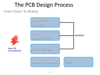
General PCB Design Considerations The basic function of a printed circuit is to provide support for circuit components and to interconnect the components electrically. In order to achieve these objectives, various printed wiring types have been developed. They vary in base material (laminate), conductor type, number of conductor planes, rigidity, etc. It is therefore expected that the printed circuit designers are adequately familiar with the variations and their effect on cost, component placement, wiring density, delivery cycles and functional performance. No finished product is ever better than its original design or the material from which it is made. The manufacturing process, at best, can reproduce the design. The same is true with printed circuit boards. The need for formalizing design and layout methods and procedures thus assumes critical importance
Design and layout broadly includes the perspective of total system hardware, which includes not only the printed circuit but each and every component in its final form. Design and layout considerations must also address the relations between and interactions of the components and assemblies throughout the system. Board design is an extremely important aspect of printed circuit board technology. Quite often, designers underestimate the time and effort required to do a good job. This can cause delay in production start-up and much hidden cost during the life of the product.
Technical Requirements The technical requirements that are likely to affect the design of an electrical equipment are mechanical, electrical, functional and environmental. Mechanical design requirements include size, shape and weight; location of components and their mounting, dimensional tolerances, shielding and equipment marking. Electrical design requirements have such parameters as circuit function and wiring distribution, component selection with respect to electrical ratings, size and tolerance, internal and external interconnections. Functional design parameters include reliability, maintainability, accessibility, and human engineering (displays, controls). Environmental design takes into account factors such as mechanical shock and vibration, temperature extremes, salt spray and fungus proofing and operations in space or underwater.
Important Design Elements The design inputs which should be provided by the equipment designer to the PCB designer are called design elements. They are: Type of circuit (analog or digital, etc.); Board size Number of layers Pad stack sizes Hole sizes Layer thickness Board thickness External connections Mounting holes Supply and ground layer thickness and Component details with specifications.
Important Performance Parameters Tensile strength; Flexural strength; Shock and vibration; Thermal shock and temperature cycling; Moisture resistance; Fungus resistance; Salt spray; Warp or twist; Dielectric breakdown voltage; Solderability and re-solderability; Insulation resistance (surface and bulk); Flame resistance; Conductor temperature rise; Machinability; and High attitude considerations.
Mechanical Design Considerations Types of Boards Board Mounting Techniques Board Guiding and Retaining Input/Output Terminations Board Extraction Testing and Servicing Mechanical Stress Board Thickness Important Specifications and Standards
Electrical Design Considerations Conductor Dimensions Resistance Capacitance Considerations Inductance of PCB Conductors High Electrical Stresses
Fabrication and Assembly Considerations Certain limits should be taken into account in order to maximize manufacturability and thereby minimize cost. Also, the human factors should be considered before designing is undertaken. These factors are delineated below. Conductor spacing less than 0.1mm will not work with the etching process, because the etchant fluid does not circulate efficiently in narrower spaces resulting in incomplete metal removal. Features with a conductor width smaller than 0.1 mm will lead to breakage and damage during etching. The land size should be at least 0.6 mm greater than the hole size.
The following limitations determine the layout techniques: Size capability of reprographic camera for film master production; Artwork table size; Minimum or maximum board processing size; Drilling accuracy; and Fine line etching facilities.
The following parameters are taken into considerations for design from the point of view of assembly of printed circuit boards: Hole diameter shall be expressed in terms of maximum material conditions (MMC) and least material conditions (LMC) limits. Properly locate smaller components so that they are not shadowed by large components. Solder mask thickness should not be greater than 0.05 mm. Screen print legend must not interface with any solder pad. The top half of the board should be a mirror of the bottom half of the board to achieve a balanced construction, because asymmetrical boards tend to warp.
Design Rules for Analog Circuits The three important considerations which form the basis for design rules for analog circuit PCBs are: Component placement; Signal conductors; and Supply and ground line conductors.
Component Placement Component placement plays a crucial role, especially in analog circuits PCB design. The important guidelines to be followed in this regard are: Components which need to be accessed from the front panel must be placed exactly according to the requirements of the equipment designer. Components for internal adjustments such as potentiometers, trimmers, switches, etc. should be arranged near the board edge and placed in the proper direction for easy operation. Components with metal cases should not be placed very near to potentiometers, trimmers and switches etc. otherwise while adjusting, the screwdriver may cause a short-circuit between the component and the equipment chassis. The placing of heat-producing and heat-sensitive components must be carefully planned. Heat producing components should be placed away from the heat-sensitive components. Heat-producing components should be uniformly distributed over the entire board area as far as possible. This will avoid local over-heating of the board. Components likely to get heated must be separated from the board surface by suitable spacers. Provision for space for these spacers should be made on the board. Where mounting screws need to be provided, the requisite space for nut and washer must be planned for, and no conductive track should be run underneath.
Signal Conductors Signal conductors in analog circuit PCBs have to perform a variety of different tasks including input, reference level, feedback, output, etc. Therefore, a signal line for one application has to be optimized in a different manner than for another application. But a common consideration in all analog circuit PCB designs is to keep the signal conductor as short as possible. This is because the magnitude of the undesirable inductive and capacitive coupling effects increases almost proportionally to the length of the signal conductor. It may not always be possible to keep all signal conductors as short as possible. A practical approach in such a case is to identify the most critical signal conductor and to put it first in the layout. The signal conductor layout has to be made carefully, particularly for the following types of circuits: High frequency amplifiers/oscillators; Multi-stage amplifiers especially with high power output stage; High gain dc amplifiers; Low level signal amplifiers; and Differential amplifiers.
Supply and Ground Conductors Power supply lines should be of sufficient width to keep the resistance and inductance to a low value. However, the capacitive coupling to ground increases with more width. Analog and digital circuits on the same PCB should strictly have independent ground network conductors. Similarly, reference voltage circuits, which are normally sensitive to ground potential fluctuations, should tap the supply lines directly at the input to the PCB and its ground line should be connected separately to the stable ground reference point of the equipment. In real life, ground conductors have both resistance and inductance, and may also be carrying unpredictable currents, which will have voltage drops when they flow in the ground impedances. CAD PCB programs are particularly bad at ground design because they tend to keep all conductors as thin as possible to conserve copper and the board area, and this, of course, results in high ground resistance. There is an obvious alternative to thin ground leads a continuous ground plane of copper covering one side of a PCB to which all ground connections are made. The resistance of 0 .001" (0.025 mm) copper is approximately 0.67 mW/square inch so that this solution is frequently adequate but not always.
General Rules for Design of Analog PCBs A few general rules concerning design of PCBs for analog circuits are: Keep the signal path as short as possible. This will help to minimize both voltage drops through the conductors as well as electromagnetic interference by controlling loop areas. Provide separate analog and digital grounds and tie the two together only once. Provide one connection from the system ground to the actual earth ground. Connect capacitive shields once to provide a return path to the noise source. Magnetic shields must be made out of a highly permeable material to be effective. Metal should not be left electrically floating. Maintain the balance of a system to prevent common mode signals from becoming differential. Limit the bandwidth of the system to the required signal bandwidth. Keep loop areas small and always think as to where the currents will flow. Between the two PCBs, use twisted pair cable to improve the noise rejection of a system.
Design Rules for Digital Circuits Until recently, the only task printed circuit boards were expected to perform was to provide electrical connectivity between various components and the conductors had to be of sufficient cross-sectional area to tolerate the necessary current without excessive over-heating. The conductor separation was so arranged that it should prevent voltage breakdown. The widespread use of digital integrated circuits has now resulted in devices with extremely fast switching speeds and rise times. Electromagnetic wave propagation characteristics have become important and need to be considered carefully. Under these circumstances, the printed circuit boards may act as transmission lines if the rise or fall time of the driving device is less than twice the propagation delay. It is essential to understand that it is the rise/fall time that is critical and not the operating frequency However, the frequency is dependent on rise/fall times, since the lower the value of the rise/fall time, the faster the operating frequency of the device. Under these situations, the transmission line effects become applicable and knowledge of the electrical characteristics associated with the conductors acting as transmission lines is essential. Then, the characteristic impedance must be matched to that of the receiving device to prevent reflection.
Problems in Design of PCBs for Digital Circuits High frequency performance of printed circuit boards is becoming increasingly important in digital circuits and knowledge of electrical characteristics associated with conductors acting as transmission lines is essential The main problems that can affect digital PCBs, if they are not properly designed; are: Reflections (causing signal delays and double pulsing, i.e. conversion of one pulse into two or more pulses); Cross-talk (interference between neighbouring signal lines); Ground and supply signal noise; and Electromagnetic interference from pulse type electromagnetic fields.
Connectivity in electronic equipment Electronic equipment is a combination of electrical and electronic components connected to produce a certain designed function. In the era of vacuum tubes and even later, electronic equipment was constructed by hand wiring and by point-to-point soldering. The wires were stripped of their insulation, tinned and soldered. Each discrete component was installed by hand, electrically and mechanically. The equipment was obviously large, awkward and bulky. It was difficult to meet the demanding requirements for the use of this equipment in aircrafts, the health sector and home emergency uses, thereby necessitating the development of smaller and more compact electronic equipment. A natural evolution took place in several areas. Smaller components were developed and modular design became popular, basically intended to decrease the time between unit failure and repair due to easy replaceability. The use of miniaturization and sub-miniaturization in electronic equipment design gave birth to a new technique in inter-component wiring and assembly that is popularly known as the printed circuit board. The printed circuit board provides both the physical structure for mounting and holding electronic components as well as the electrical interconnection between components. Printed circuit board is usually abbreviated as PCB and quite often referred to as board. However, in the USA, the term PWB (Printed Wiring Board) is more often used instead of PCB.
Advantages of Printed Circuit Boards Advantages of Printed Circuit Boards There are many good reasons for using printed circuit boards instead of other interconnection wiring methods and component mounting techniques, some of which are as follows: The size of component assembly is reduced with a corresponding decrease in weight. Quantity production can be achieved at lower unit cost. Component wiring and assembly can be mechanized. Circuit characteristics can be maintained without introducing variation in inter-circuit capacitance. They ensure a high level of repeatability and offer uniformity of electrical characteristics from assembly to assembly. The location of parts is fixed, which simplifies identification and maintenance of electronic equipment and systems. Inspection time is reduced because printed circuitry eliminates the probability of error. Printed wiring personnel require minimal technical skills and training. Chances of mis- wiring or short-circuited wiring are minimized.
Components of a Printed Circuit Board The essential components of a printed circuit board are: The base, which is a thin board of insulating material, rigid or flexible, which supports allconductors and components; and The conductors, normally of high purity copper in the form of thin strips of appropriate shapes firmly attached to the base material. The base provides mechanical support to all copper areas and all components attached to the copper. The electrical properties of the completed circuit depend upon the dielectric properties of the base material and must therefore, be known and appropriately controlled. The conductors provide not only the electrical connections between components but also solderable attachment points for the same. When the completed board provides mechanical support and all necessary electrical connections to the components, it is essentially a Printed Wiring Board or Printed Circuit Board. The term printed became popular because the conductive areas are usually generated by means of a printing process like screen printing or photo-engraving, which are commonly used to print drawings or inscriptions.
Classification of Printed Circuit Boards Printed Circuit Boards may be classified according to their various attributes, often with ambiguous results. They were traditionally divided into three classes according to their use and applications, and were commonly referred to as 1. consumer, 2. professional and 3. high reliability boards.
Consumer PCBs were generally used in consumer products such as radio, television, and cheap test and measuring equipment. They used less expensive base material and allowed greater tolerances for manufacture to keep the cost low. Much importance was not given to good and consistent electrical properties. Professional boards were made of better quality material to achieve tighter electrical and environ- mental specifications using controlled fabrication techniques. Higher reliability boards, normally used in strategic applications, were meant to provide the best of electrical properties through the use of high quality base material and tightly controlled manufacturing processes.
A more simple and understandable classification is now used, which is based on the number of planes or layers of wiring, which constitute the total wiring assembly or structures, and to the presence or absence of plated- through holes. This method of classifying boards has the advantage of being related directly to the board specifications. The above classification might have been applicable two or three decades ago, but presently, the distinction between consumer and professional markets has disappeared. Many consumer products like compact discs, camcorders or cameras have become more complex, reliable and demanding than what was hitherto considered as professional equipment like personal computers. The advent of surface mount technology and developments in automatic assembly techniques requires that the boards even for the cheapest product must be manufactured to strict mechanical tolerances.
Single-sided Printed Circuit Boards Single-sided means that wiring is available only on one side of the insulating substrate. The side which contains the circuit pattern is called the solder side whereas the other side is called the component side . These types of boards are mostly used in case of simple circuitry and where the manufacturing costs are to be kept at a minimum. The single-sided boards are manufactured mostly by the print and etch method or by the die- cut technique by using a die that carries an image of the wiring pattern; and the die is either photo- engraved or machine- engraved. Normally, components are used to jump over conductor tracks, but if this is not possible, jumper wires are used. The number of jumper wires on a board cannot be accepted beyond a small number because of economic reasons, resulting in the requirement for double-sided boards.
Double Double- -sided Printed Circuit Boards sided Printed Circuit Boards Double-sided printed circuit boards have wiring patterns on both sides of the insulating material, i.e. the circuit pattern is available both on the components side and the solder side. Obviously, the component density and the conductor lines are higher than the single-sided boards. Two types of double- sided boards are commonly used, which are: 1. Double-sided board with plated through-hole connection (PTH); and 2. Double-sided board without plated through-hole connection (non-PTH).
Double-sided PTH board Double-sided PTH board has circuitry on both sides of an insulating substrate, which is connected by metallizing the wall of a hole in the substrate that intersects the circuitry on both sides. This technology, which is the basis for most printed circuits produced, is becoming popular in cases where the circuit complexity and density is high. Figure shows the configuration of a plated through-hole in a printed circuit board.
Double-sided non-PTH board Double-sided non-PTH board is only an extension of a single-sided board. Its cost is considerably lower because plating can be avoided. In this case, through contacts are made by soldering the component leads on both sides of the board, wherever required. In the layout design of such boards, the number of solder joints on the component side should be kept to a minimum to facilitate component removal, if required. It is generally recommended that conductors should be realized as much as possible on the non-component side and only the remaining should be placed on the component side.
The non-plating technique in double-sided boards is shown in Figure 1.3 wherein the interconnection is made by a jumper wire. A formed insulated solid lead wire is placed through the hole, clinched and soldered to the conductor pad on each side of the board.
Different types of eyelets are also used for double-sided board interconnection. These are illustrated
Multi-layer Boards The development of plated through-hole technology has led to a considerable reduction in conductor cross-overs on different planes, resulting in a reduction in space requirements and increased packaging density of electronic components. However, the modern VLSI and other multi-pin configuration devices have tremendously increased the packaging density and consequently the concentration of inter-connecting lines. This has given rise to complex design problems such as noise, cross- talk, stray capacitances and unacceptable voltage drops due to parallel signal lines. These problems could not be satisfactorily solved in single-sided or double-sided boards, thereby necessitating an extension of the two- plane approach to the multi-layer circuit board.
A multi-layer board is, therefore, used in situations where the density of connections needed is too high to be handled by two layers or where there are other reasons such as accurate control of line impedances or for earth screening. The multi-layer board makes use of more than two printed circuit boards with a thin layer of what is known as prepreg material placed between each layer, thus making a sandwich assembly as shown in Figure 1.5. The printed circuit on the top board is similar to a conventional printed circuit board assembly except that the components are placed much closer to avoid having many terminals, which necessitates the use of additional board layers for the required interconnections. The electrical circuit is completed by interconnecting the different layers with plated through-holes, placed transverse to the board at appropriate places. Multi-layer boards have three or more circuit layers, while some boards have even as many as 50 layers. By virtue of the multi-layer conductor structure, multi-layer printed wiring has facilitated a reduction in the weight and volume of the interconnections commensurate with the size and weight of the components it interconnects.
Two types of multi-layer boards, one with four-layers & the other with eight-layers.
Application The following areas of application necessitate the use of multi-layer printed wiring arrangements: Wherever weight and volume savings in interconnections are the overriding considerations, as in military and air-borne missile and space applications; When the complexity of interconnection in sub-systems requires complicated and expensive wiring or harnessing; When frequency requirements call for careful control and uniformity of conductor wave impedances with minimum distortions and signal propagation, and where the uniformity of these characteristics from board-to- board is important; When coupling or shielding of a large number of connections is necessary; the high capacitance distributed between the different layers gives a good de-coupling of power supply which permits satisfactory operation of high speed circuits; With multi-layers, all interconnections can be placed on internal layers, and a heat sink of thick solid copper can be placed on the outer surfaces. By mounting the components directly on the metallic surfaces, the problem of heat distribution and heat removal in systems can be minimized. Also, the layout and artwork designs are greatly simplified on account of the absence of the supply and ground lines on the signal planes
Rigid and Flexible Printed Circuit Boards Printed circuit boards can also be classified on the basis of the type of insulating material used, i.e. rigid or flexible. While rigid boards are made of a variety of materials, flexible boards use flexible substrate material like polyester or polyamide. The base material, which is usually very thin, is in the range of 0.1 mm thickness. Laminates used in flexible boards are available with copper on one or both sides in rolls. Rigid-flex boards, which constitute a combination of rigid and flexible boards usually bonded together, are three-dimensional structures that have flexible parts connecting the rigid boards, which usually support components. This arrangement gives volumetrically efficient packaging and is therefore gaining widespread use in electronic equipment. Flexible PCBs may be single-sided, double-sided (PTH or non-PTH) or multi-layer.
A variety of processes are currently used for manufacturing printed circuit boards. However, most of the processes have identical or similar basic steps. Variations in the basic manufacturing steps are usually made by the manufacturers to improve quality or specific yield. The most popular process is the print and etch method, which is a purely subtractive method. In this process, the base material used is copper clad laminate to which all the electronic components are soldered, with one or more layers of etched metal tracks making the connection. The etching process involves achieving a conductive pattern formed on one or both sides of the laminate. The term printed wiring or printed circuit refers only to the conductive pattern that is formed on the laminate to provide point-to-point connection. Four specific phases of the PCB manufacturing process need to be understood. These are design, fabrication, assembly and test.