PCB Design Tutorial Steps & Interactions

Learn the step-by-step process of designing a PCB, from breaking down functionality into modules to creating the system schematic, wiring connections, and PCB layout. Discover tips for component selection, interaction with schematic parts, and ensuring proper design rules are followed.

Download Presentation

Please find below an Image/Link to download the presentation.
The content on the website is provided AS IS for your information and personal use only. It may not be sold, licensed, or shared on other websites without obtaining consent from the author. Download presentation by click this link. If you encounter any issues during the download, it is possible that the publisher has removed the file from their server.
E N D
Presentation Transcript
Eagle PCB Tutorial Josh Fromm EE 475, April 11th
Steps in Designing a PCB > Decide what functionality you need Break that functionality into small modules > Sense motion -> IMU > Communicate with phone -> Bluetooth module Research components for each module > Always read the datasheets > Check to make sure footprints are solderable Choose a CPU that can interface with your modules and meets other requirements > Try not to pick something overly complicated
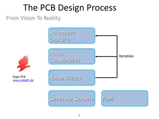
Steps in Designing a PCB > Make the system schematic Confirm every part has a schematic symbol and footprint > If it doesn t then make your own Place all parts on the schematic and wire Remember to add lots of bypass caps Check errors to make sure everything is properly connected > Make PCB Check design rules Place parts in reasonable location (minimize rats nest) Use polygon pours for power and ground Route remaining traces (use larger width for high current) Check DRC
Interacting with Schematic Parts > All parts have a crosshair that can be interacted with > Kind of goofy for some parts like frame > When selecting multiple objects, some commands like move require right clicking to affect the whole group
Wiring it Up > Use net tool to make connections > Don t always need to make a physical connection Create a partial net Use the name tool to give it a proper name Use the label tool to place that name right on the net Repeat for other pins you want to connect > Always do an ERC when finished to find any mistakes.
PCB Layout > Use File -> switch to schematic to create a PCB for your schematic > First set up your grid, usually want a slightly large grid and a much smaller alt grid > Next, use DRC to set up design rules according to PCB manufacturer requirements Can download and import Osh Park DRU > When moving parts, everything snaps to grid, can hold ALT key to get more fine grained control > Try to arrange parts to minimize the rat s nest
Routing > Current operating layer shown in upper left > Click middle mouse button to switch > Focus on one trace at a time Use middle click to place a via Right click to change wire style For tight boards, try to keep top layer horizontal and bottom layer vertical Use bigger traces for power and ground if possible > When finished, use rats nest to check if anything missed > Always do a DRC
Advanced Routing > Good idea to use polygon pours for Power and Ground Provides good capacitance to reduce noise Makes routing easier Looks cool > Use polygon pour tool to trace outline > Press ratsnest to fill in. > Can still route through the pour or hide with ripup on the edge > Also fun to write on the board by editing the silkscreen Choose tPlace or bPlace layer then use drawing or text tools Wont affect circuit, purely visual
Finishing Up > Need to convert schematic to format a PCB manufacturer can parse Standard to use Gerber files Need one Gerber file for each layer of the board > Press the Cam tool button Open job, choose the sparkfun job file Process job Zip the cam files up and submit to Osh Park
Creating Custom Parts > From the Control Panel go to File -> New -> Library > Library -> Symbol, name it and accept > This opens an editor similar to a schematic Use shapes to draw a box Use the add pins tool to place pins on the box Name the pins Good idea to add >NAME and >VALUE text to part to allow more customization down the line, make sure to set these to Names and Values layer respectively Save and then go to Library -> Create -> Package
Creating Custom Footprints > Start by using the SMD or pad tool to place pads > Can change to metric units using grid > Set size of pads with info tool > The grid is your friend Set the grid distance to be the distance between pads for quick and easy placement Hold control while moving to have pads center on grid Can also use info to explicitly choose center > Use tPlace layer to draw shape of chip body (optional) > Add >NAME and >VALUE text in tName and tValue layers
Associate Symbol and Package > Library -> Device -> New Name it the same thing as the Symbol and Package > Use add to place the symbol for the part > In the right side, press new and add the Package Note the yellow exclamation, this means pins have not been associated > Double click on the package name to associate > Set prefix (default is U) > Match left and right sides then press connect > Save and you re done! > Find your library in the control panel, right click and use