Logic Minimization Techniques Using Karnaugh Maps
Learn about Karnaugh Maps, an efficient tool for logic minimization, and how to apply them for minimizing Boolean functions using different forms and steps. Understand the goals of minimization and alternate methods to optimize circuit design efficiently.

Download Presentation

Please find below an Image/Link to download the presentation.
The content on the website is provided AS IS for your information and personal use only. It may not be sold, licensed, or shared on other websites without obtaining consent from the author. If you encounter any issues during the download, it is possible that the publisher has removed the file from their server.
You are allowed to download the files provided on this website for personal or commercial use, subject to the condition that they are used lawfully. All files are the property of their respective owners.
The content on the website is provided AS IS for your information and personal use only. It may not be sold, licensed, or shared on other websites without obtaining consent from the author.
E N D
Presentation Transcript
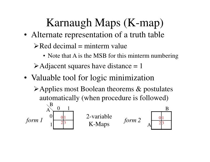
Karnaugh Maps (K-map) Alternate representation of a truth table Red decimal = minterm value Note thatAis the MSB for this minterm numbering Adjacent squares have distance = 1 Valuable tool for logic minimization Applies most Boolean theorems & postulates automatically (when procedure is followed) B A 0 1 K-Maps 0 1 B 2-variable 0 1 2 3 0 1 2 3 form 1 form 2 A
Karnaugh Maps (K-map) Alternate forms of 3-variable K-maps Note end-around adjacency Distance = 1 Note:Ais MSB, C is LSB for minterm 00 numbering C 0 1 AB 0 1 2 3 01 BC A 0 1 00 01 11 10 11 6 7 4 5 form 1 3 2 7 6 0 1 4 5 10 C B 0 1 2 3 form 2 3 2 7 6 0 1 4 5 B A 6 7 4 5 A C
K-mapping & Minimization Steps Step 1: generate K-map Put a 1 in all specified minterms Put a 0 in all other boxes (optional) Step 2: group all adjacent 1s without including any 0s All groups (aka prime implicants) must be rectangular and contain a power-of-2 number of 1s 1, 2, 4, 8, 16, 32, An essential group (aka essential prime implicant) contains at least 1 minterm not included in any other groups A given minterm may be included in multiple groups Step 3: define product terms using variables common to all minterms in group Step 4: sum all essential groups plus a minimal set of remaining groups to obtain a minimum SOP
K-map Minimization Example Z= A,B,C(1,3,6,7) Recall SOP minterm implementation 8 gates 27 gate I/O K-map results 4 gates 11 gate I/O Note: this group not needed since 1s are already covered Row value BC A 0 1 00 0 01 1 11 1 10 0 A B C 0 0 0 0 0 1 0 1 1 0 1 0 1 1 0 1 1 Z 0 1 0 1 0 0 1 1 0 1 0 1 0 1 0 1 2 3 4 5 6 7 32 0 1 04 17 61 50 essential prime implicants A A C B A C Z=AC +AB 1 AB
K-map Minimization Goals Larger groups: Smaller product terms Fewer variables in common SmallerAND gates In terms of number of inputs Fewer groups: Fewer product terms FewerAND gates Smaller OR gate In terms of number of inputs Alternate method: Group 0s Could produce fewer and/or smallerproduct terms Invert output Use NOR instead of OR gate
4-variable K-maps Note adjacency of 4 corners as well as sides Variable ordering for this minterm numbering:ABCD CD AB 00 01 11 10 00 0 1 3 2 4 5 7 6 C 0 1 4 5 3 2 7 6 01 B 11 12 13 8 9 15 14 11 10 12 13 8 9 15 14 11 10 A 10 D form 1 form 2
5-variable K-map Note adjacency between maps when overlayed distance=1 Variable order for this minterm numbering: A,B,C,D,E (A is MSB, E is LSB) BCDE00 BCDE00 01 11 10 01 11 10 00 00 16 17 20 21 3 2 7 6 0 1 4 5 19 18 23 22 01 01 11 11 31 30 27 26 28 29 24 25 15 14 11 10 12 13 8 9 10 10 A=1 A=0
5-variable K-map Changing the variable used to separate maps changes minterm numbering Same variable order for this minterm numbering: A,B,C,D,E (A is MSB, E is LSB) ABCD00 ABCD00 01 11 10 01 11 10 00 00 6 4 14 12 0 2 8 10 1 3 9 11 7 5 15 13 01 01 11 11 31 29 23 21 25 27 17 19 30 28 22 20 24 26 16 18 10 10 E=1 E=0
6-variable K-map Variable order for minterm numbers:ABCDEF CDEF00 CDEF00 01 11 10 01 11 10 00 00 16 17 20 21 3 2 7 6 0 1 4 5 19 18 23 22 01 01 A=0 11 11 31 30 27 26 28 29 24 25 15 14 11 10 12 13 8 9 10 10 CDEF00 CDEF00 01 11 10 01 11 10 00 00 48 49 52 53 51 50 55 54 35 34 39 38 32 33 36 37 01 01 A=1 11 11 63 62 59 58 60 61 56 57 47 46 43 42 44 45 40 41 10 10 B=1 B=0
Dont Care Conditions Sometimes input combinations are of no concern Because they may not exist Example: BCD uses only 10 of possible 16 input combinations Since we don t care what the output, we can use these don t care conditions for logic minimization The output for a don t care condition can be either 0 or 1 WE DON T CARE!!! Don t Care conditions denoted by: X, -, d, 2 X is probably the most often used Can also be used to denote inputs Example:ABC = 1X1 =AC B can be a 0 or a 1
Dont Care Conditions TruthTable K-map Minterm Z= A,B,C(1,3,6,7)+d(2) Maxterm Z= A,B,C(0,4,5)+d(2) Notice Don t Cares are same for both minterm & maxterm A A C B A B C 0 0 0 0 0 1 0 1 1 0 1 0 1 1 1 1 Z 0 1 X 1 0 0 1 1 BC A 0 1 00 0 01 1 11 1 10 X 0 1 0 1 0 1 0 1 3 2 0 1 04 17 61 50 Z=B+A C A C Circuit analysis: G=3 (compared to G=4 & GIO=11 w/o don t care) Z=AC + B GIO=8
Design Example Hexadecimal to 7-segment display decoder Acommon circuit in calculators 7-segments (A-G) to represent digits (0-9 &A-F) Alogic 1 turns on given segment A B F G E C D active (on) segments for a given HEX value A B C D F F 7 segments In3 In2 Hex to 7-segment decoder = don t care In1 In0 Circuit block diagram
HEX to 7-seg Design Example Create truth table from specification In3 In2 In1 In0 0 0 0 0 0 0 0 0 0 1 0 1 0 1 0 1 1 0 1 0 1 0 1 0 1 1 1 1 1 1 1 1 A 1 0 1 1 0 1 1 1 1 1 1 0 1 0 1 1 B 1 1 1 1 1 0 0 1 1 1 1 0 0 1 0 0 C 1 1 0 1 1 1 1 1 1 1 1 1 0 1 0 0 D 1 0 1 1 0 1 1 0 1 X 0 1 1 1 1 0 E 1 0 1 0 0 0 1 0 1 0 1 1 1 1 1 1 F 1 0 0 0 1 1 1 X 1 1 1 1 1 0 1 1 G 0 0 1 1 1 1 1 0 1 1 1 1 0 1 1 1 A 0 0 1 1 0 0 1 1 0 0 1 1 0 0 1 1 0 1 0 1 0 1 0 1 0 1 0 1 0 1 0 1 B F G E C D = don t care
HEX to 7-seg Design Example Generate K-maps & obtain logic equations In1In0 00 1 01 0 11 1 10 1 In3 In2 In3 In2 In1 In0 A 0 0 0 0 0 0 0 0 0 1 0 1 0 1 0 1 1 0 1 0 1 0 1 0 1 1 1 1 1 1 1 1 B 1 1 1 1 1 0 0 1 1 1 1 0 0 1 0 0 C 1 1 0 1 1 1 1 1 1 1 1 1 0 1 0 0 D 1 0 1 1 0 1 1 0 1 0 0 1 1 1 1 0 E 1 0 1 0 0 0 1 0 1 0 1 1 1 1 1 1 F 1 0 0 0 1 1 1 0 1 1 1 1 1 0 1 1 G 0 0 1 1 1 1 1 0 1 1 1 1 0 1 1 1 00 0 0 1 1 0 0 1 1 0 0 1 1 0 0 1 1 0 1 0 1 0 1 0 1 0 1 0 1 0 1 0 1 1 0 1 1 0 1 1 1 1 1 1 0 1 0 1 1 K-map for Aoutput 0 1 1 1 01 1 0 1 1 11 1 1 0 1 10 A= In2 In0 + In3 In1 + In2 In1 + In3 In0 + In3 In2 In0 + In3 In2 In1 In1In0 In3 In2 00 00 1 01 1 11 1 10 1 K-map for B output 1 0 1 0 01 0 1 0 0 11 1 1 0 1 10 B = In2 In0 + In2 In1 + In3 In1 In0 + In3 In1 In0 + In3 In1 In0
HEX to 7-seg Design Example K-maps & logic equations for outputs C-G In1 In0 In1 In0 In1In0 In1In0 00 1 01 0 11 0 10 0 00 1 01 1 11 1 10 0 00 1 01 0 11 1 10 1 00 1 01 0 11 0 10 1 In3In2 In3In2 In3 In2 In3In2 00 00 00 00 1 1 1 1 0 1 0 1 1 1 X 1 0 0 0 1 01 01 01 01 0 1 0 0 1 1 0 1 1 0 1 1 1 1 1 1 11 11 11 11 1 1 1 1 1 0 1 1 1 1 1 1 1 X 1 0 10 10 10 10 K-map for E output K-map for C output K-map for D output K-map for F output In1In0 C = In3 In2 + In1 In0 + In2 In1 + In3 In0 + In3 In2 D = In3 In2 In0 + In2 In1 In0 + In2 In1 In0 + In3 In1 + In2 In1 In0 E = In2 In0 + In3 In2 + In1 In0 + In3 In1 F = In1 In0 + In3 In2 + In2 In0 + In3 In1 + In3 In2 G = In3 In2 + In1 In0 + In3 In0 + In3 In2 In1 + In2 In1 00 0 01 0 11 1 10 1 In3 In2 00 1 1 0 1 01 0 1 1 1 11 1 1 1 1 10 K-map for G output
HEX to 7-seg Design Example Remaining steps to complete design: Draw logic diagram (sharing common gates) Analyze for optimization metirc: G, GIO, Gdel, Pdel See next page for logic diagram & circuit analysis Simulate circuit for design verification Debug & fix problems when output is incorrect Check truth table against K-map population Check K-map groups against logic equation product terms Check logic equations against schematic Optimize circuit for area and/or performance Use Boolean postulates & theorems Re-simulate & verify optimized design
#loads on PIs 9 In3 9 In2 9 In1 HEX to 7-seg Design Example In3 In0 In3 In2 In3 In1 1+9 2+3 G1 In2 2+1 In3 In1 In3 In2 3+1 In0 In2 In1 3+1 In0 In3 1+8 In2 1+7 In1 1+9 G1 G2 G3 G4 G17 G18 Prop delay in gates #inputs + # loads In3 In1 In0 In3 In1 In0 2+1 G10 G20 3+1 6+0 A G1 G5 G19 G20 G21 C G22 G23 G24 G25 G26 E G6 G11 G12 G13 G16 G 2+2 G11 9 3+1 G21 In0 In2 In0 In3 In1 In2 In1 In3 In0 In2 In1 In3 In2 In1 In0 In3 In2 In1 In0 In0 5+0 B 2+2 G12 G6 G7 G5 G10 G11 G13 2+1 G22 5+0 In0 In3 In0 In2 In1 In1 In0 In3 In2 In0 In3 2+1 G2 2+1 G14 G23 5+0 D 2+1 G3 2+1 G15 G1 G8 G9 G12 G4 2+1 4+0 G24 2+1 G16 G5 2+1 In2 5+0 F 3+1 G17 In1 3+2 G25 2+3 G6 G6 G9 G14 G15 G27 In0 In2 5+0 2+1 G7 3+1 G18 In1 3+1 In2 In1 In3 In1 In0 G26 CircuitAnalysis G = 38 Gdel= 3 worst case path: In0 In0 G1 A In0 In3 In2 In1 GIO= 141 Pdel= 30 2+1 G8 3+1 3+1 G19 G27 G9 2+1
")
")