Thermal Analysis of a Bipolar Transistor Using COMSOL
Thermal Analysis of a Bipolar Transistor
COMSOL
Section 1
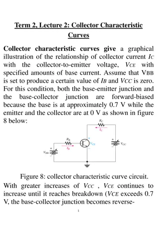
In this model, the heat transfer in solids interface is added and configured to calculate the
temperature distribution throughout the device
The Semiconductor interface provides the heat source used in the heat transfer in Solids
interface; whilst the temperature distribution that is used in the semiconductor interface
is calculated by the heat transfer in solids interface
Model Definition
Geometry 1
Model Definition
Semiconductor
Model Definition
Heat Transfer in Solids
Results
The figure is the Gummel plot,
which shows the collector and
base currents, plotted on a
logarithmic y-axis as a function of
the base voltage
The two datasets are nearly
identical because the temperature
throughout the device in the fully
coupled study does not deviate
more than a few degrees from the
T0 value used in the initial study
Gummel plot showing the collector and base currents as a function of
base voltage
Results
The figure shows the current gain
curve, which is the ratio of the
collector to base current, as a
function of the base voltage
The small magnitude of the base
current for low values of the
collector current lead to some
numerical instability for collector
currents less than approximately 10-
10 A
Again, the two datasets are similar
due to the small temperature
difference between the initialization
study and the fully coupled study
Current gain curve showing the ratio of collector to base current as a
function of base voltage
Results
The figure shows the
semiconductor heat source
This is the heat source that is
used by the heat transfer in solids
interface to calculated the
temperature distribution
throughout the device
Semiconductor heat source for a base voltage of 1.1 V and a collector
voltage of 3 V
Results
The figure shows the voltage and
temperature throughout the device
The top surface plot shows the voltage
distribution, along with the electron and
hole currents as black and white arrow
plots, respectively
As expected, the hole current is between
the base and emitter contacts, without
entering the collector region, whilst the
electron current is predominantly between
the collector and emitter
The lower surface plot shows the
corresponding temperature throughout the
device, along with an arrow plot which
shows the heat flux
Voltage and temperature for a base voltage of 1.1 V and a collector
voltage of 3 V. Top panel: Voltage distribution with electron and hole
currents shown in black and white arrows. Bottom panel: Corresponding
temperature throughout the device, along with the heat flux shown as
arrows
Results
The temperature is highest between the
emitter and collector contacts, at the depth
of the junction between the base and
collector regions
This is the expected result as the majority
of the current flows between these two
contacts, and the base-collector junction
creates a region with higher resistance than
the surrounding bulk material
Thus the Joule heating, which is the
predominant semiconductor heating
mechanism in this model, is largest in this
location
Semiconductor heat source for a base voltage of 1.1 V and a collector
voltage of 3 V
Results
Semiconductor heat source for a base voltage of 1.1 V and a collector
voltage of 3 V
The heat flux also behaves as expected, as
it flows from the peak temperature toward
the contacts, which are the only boundaries
that allow heat transfer in this simple
model
This model utilizes a COMSOL simulation to analyze the thermal behavior of a bipolar transistor. The heat transfer within the device is calculated to determine the temperature distribution. Various plots, such as the Gummel plot and current gain curve, illustrate the collector and base currents as functions of base voltage. The semiconductor heat source for specific base and collector voltages is also depicted.

Download Presentation

Please find below an Image/Link to download the presentation.
The content on the website is provided AS IS for your information and personal use only. It may not be sold, licensed, or shared on other websites without obtaining consent from the author.If you encounter any issues during the download, it is possible that the publisher has removed the file from their server.
You are allowed to download the files provided on this website for personal or commercial use, subject to the condition that they are used lawfully. All files are the property of their respective owners.
The content on the website is provided AS IS for your information and personal use only. It may not be sold, licensed, or shared on other websites without obtaining consent from the author.
E N D
Presentation Transcript
Section 1 In this model, the heat transfer in solids interface is added and configured to calculate the temperature distribution throughout the device The Semiconductor interface provides the heat source used in the heat transfer in Solids interface; whilst the temperature distribution that is used in the semiconductor interface is calculated by the heat transfer in solids interface
Model Definition Geometry 1
Model Definition Semiconductor
Model Definition Heat Transfer in Solids
Results The figure is the Gummel plot, which shows the collector and base currents, plotted on a logarithmic y-axis as a function of the base voltage The two datasets are nearly identical because the temperature throughout the device in the fully coupled study does not deviate more than a few degrees from the T0 value used in the initial study Gummel plot showing the collector and base currents as a function of base voltage
Results The figure shows the current gain curve, which is the ratio of the collector to base current, as a function of the base voltage The small magnitude of the base current for low values of the collector current lead to some numerical instability for collector currents less than approximately 10- 10 A Again, the two datasets are similar due to the small temperature difference between the initialization study and the fully coupled study Current gain curve showing the ratio of collector to base current as a function of base voltage
Results The figure shows the semiconductor heat source This is the heat source that is used by the heat transfer in solids interface to calculated the temperature distribution throughout the device Semiconductor heat source for a base voltage of 1.1 V and a collector voltage of 3 V
Results The figure shows the voltage and temperature throughout the device The top surface plot shows the voltage distribution, along with the electron and hole currents as black and white arrow plots, respectively As expected, the hole current is between the base and emitter contacts, without entering the collector region, whilst the electron current is predominantly between the collector and emitter Voltage and temperature for a base voltage of 1.1 V and a collector voltage of 3 V. Top panel: Voltage distribution with electron and hole currents shown in black and white arrows. Bottom panel: Corresponding temperature throughout the device, along with the heat flux shown as arrows The lower surface plot shows the corresponding temperature throughout the device, along with an arrow plot which shows the heat flux
Results The temperature is highest between the emitter and collector contacts, at the depth of the junction between the base and collector regions This is the expected result as the majority of the current flows between these two contacts, and the base-collector junction creates a region with higher resistance than the surrounding bulk material Thus the Joule heating, which is the predominant semiconductor heating mechanism in this model, is largest in this location Semiconductor heat source for a base voltage of 1.1 V and a collector voltage of 3 V
Results The heat flux also behaves as expected, as it flows from the peak temperature toward the contacts, which are the only boundaries that allow heat transfer in this simple model Semiconductor heat source for a base voltage of 1.1 V and a collector voltage of 3 V