Transistor Operation through Collector Characteristic Curves
Collector characteristic curves provide insight into the transistor's operation in various regions such as cutoff, saturation, and active. By analyzing the relationship between collector current (IC) and collector-to-emitter voltage (VCE) with base current variations, one can understand how a transistor functions as a switch. The transitions between cutoff, active, and saturation states are illustrated graphically, showing the behavior of the transistor in different biasing conditions.

Download Presentation

Please find below an Image/Link to download the presentation.
The content on the website is provided AS IS for your information and personal use only. It may not be sold, licensed, or shared on other websites without obtaining consent from the author.If you encounter any issues during the download, it is possible that the publisher has removed the file from their server.
You are allowed to download the files provided on this website for personal or commercial use, subject to the condition that they are used lawfully. All files are the property of their respective owners.
The content on the website is provided AS IS for your information and personal use only. It may not be sold, licensed, or shared on other websites without obtaining consent from the author.
E N D
Presentation Transcript
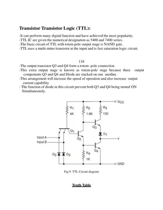
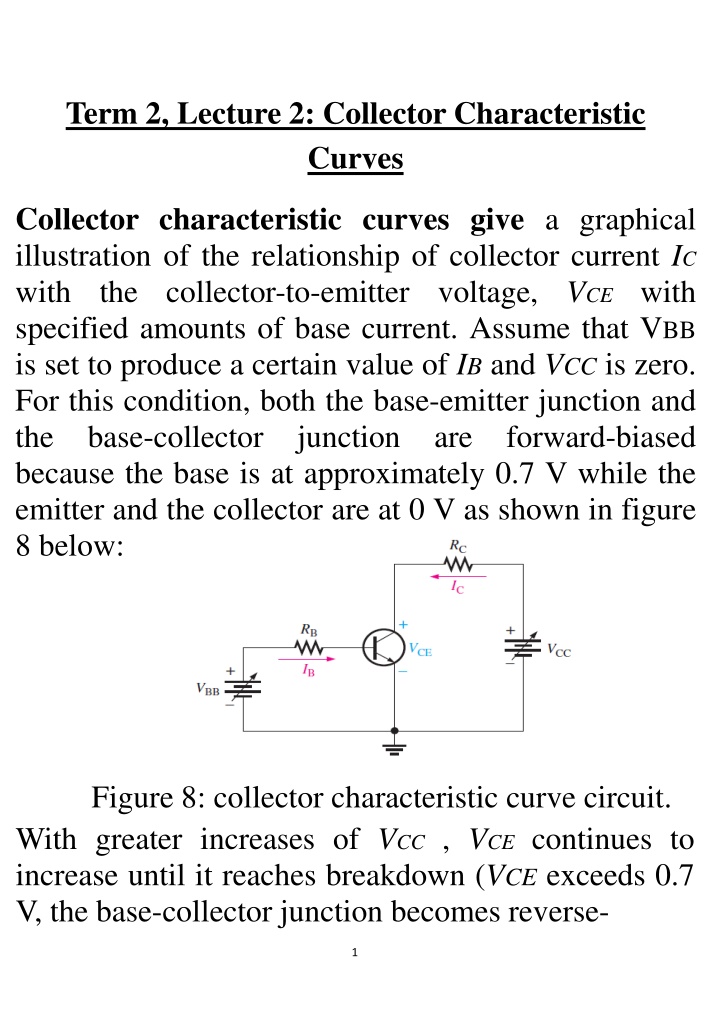
Term 2, Lecture 2: Collector Characteristic Curves Collector characteristic curves give a graphical illustration of the relationship of collector current IC with the collector-to-emitter voltage, VCEwith specified amounts of base current. Assume that VBB is set to produce a certain value of IB and VCC is zero. For this condition, both the base-emitter junction and the base-collector junction are forward-biased because the base is at approximately 0.7 V while the emitter and the collector are at 0 V as shown in figure 8 below: Figure 8: collector characteristic curve circuit. With greater increases of VCC, VCEcontinues to increase until it reaches breakdown (VCE exceeds 0.7 V, the base-collector junction becomes reverse- 1
biased and the transistor goes into the active, or linear, but the current ICremains about the same in the linear region from 0.7V to the breakdown voltage as shown in Figure 9 below: 2
Cutoff When IB = 0, the transistor is in the cutoff region of its operation. This is shown in Figure 10 with the base lead open, resulting in a base current of zero. Under this condition, there is a very small amount of collector leakage current, ICEO, due mainly to thermally produced carriers. Because ICEO is extremely small, it will usually be neglected in circuit analysis so that VCE = VCC. In cutoff, Base-emitter( Vbe < o.7V) and base-collector junctions are reverse- biased. The subscript CEOrepresents collector-to- emitter with the base open. In cutoff, the transistor appears as an open circuit between the collector and emitter terminals. Figure 10: Cutoff: Collector leakage current (ICEO) is extremely small and is usually neglected. Base-emitter and base-collector junctions are reverse-biased. 3
Saturation: As IBincreases due to increasing VBB, ICalso increases and VCEdecreases due to the increased voltage drop across RC(VCE= VCC- IC* RC). This is illustrated in Figure 11. When VCEreaches its saturation value, VCE(sat), the base-collector junction becomes forward-biased and ICcan increase no further even with a continued increase in IB.At the point of saturation, the relation is no longer valid. VCE(sat)for a transistor occurs somewhere below the knee of the collector curves. Base-emitter and base-collector junctions are forward-biased. In saturation, the transistor appears as a near short circuit between the collector and emitter terminals. Figure 11: Saturation: As IB increases due to increasing VBB, IC also increases and VCE decreases due to the increased voltage drop across RC. When the transistor reaches saturation, IC can increase no further regardless of further increase in IB. Base-emitter and base-collector junctions are forward-biased. 4
Once ICis reaches to maximum value, the transistor is said to be in saturation. Note that saturation can be determined as follows: VCE = VCC IC* RC , in saturation VCEis very small Vce <= o.2 V, assume it = 0. IC(sat) = VCC/RC Using the two states of cutoff and saturation, the transistor can used as a switch. DC Load Line Cutoff and saturation can be illustrated in relation to the collector characteristic curves by the use of a load line. Figure 12 shows a dc load line connecting the cutoff point and the saturation point. The bottom of the load line is at ideal cutoff where IC = 0 and VCE= VCC. The top of the load line is at saturation where IC = Ic(sat)and VCE= VCE(sat). In between cutoff and saturation along the load line is 5
the active or linear region of the transistor operation. Figure 12: DC load line on a family of collector characteristic curves illustrating the cutoff and saturation conditions. Example: 6
Review Questions: 1. What two variables are plotted on a collector characteristic curve? 2. What bias conditions must exist for a transistor to operate in cutoff region? 3. Explain the cutoff region? 4.What bias conditions must exist for a transistor to operate in saturation region? 5. Explain the saturation region? 6. For a given type of transistor, can beta dc be considered to be a constant? 7