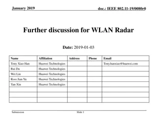
Microwave and Radar Engineering


MICROWAVE & RADAR
ENGINEERING
I
n
t
r
od
u
ction
Microwaves
are
a
form
of
electromagnetic
radiation
with
wavelengths
ranging
from
about
one
meter
to
one millimeter;
with
frequencies
between
300
MHz
(1
m)
and
300
GHz
(1
mm).
2
A
more
common
definition
in
radio
engineering
is the
range
between
1
and
100
GHz
(wavelengths
between
0.3
m
and
3
mm).
M
icrowaves
include
the
entire
SHF
band
(3
to
30
GHz,
or
10
to
1
cm)
at
minimum.
Frequencies
in
the
microwave
range
are
often
referred
to
by
their IEEE
radar
band
designations:
L,
S,
C,
X,
K
u
,
K, or
K
a
ban
D.
prefix
micro-
in
microwave
is
not meant
to
suggest
a
wavelength
in
the
micrometer
range.
Rather,
it
indicates
that
microwaves
are
"small"
(having
shorter
wavelengths),
compared
to
the
radio
waves
used prior
to
microwave
technology.
The
boundaries
between
far
infrared,
terahertz
radiation,
microwaves,
and
ultra-high-frequency
radio
waves
are
fairly
arbitrary
and
are
used
variously
between
different
fields
of
study.
Microwaves
travel
by
line-of-sight;
unlike
lower
frequency
radio
waves
they
do
not
diffract
around
hills,
follow
the
earth's
surface
as
ground
waves,
or
reflect
from
the
ionosphere.
so
terrestrial
microwave
communication
links
are
limited
by
the
visual
horizon
to
about
40
miles
3
Microwave
spectrum
4
MICROWAVE
BANDS
5
6
ADVANTAGES
OF
MICROWAVES
Large Bandwidth
: The
Bandwidth
of
Microwaves
is
larger
than
the
common low
frequency
radio
waves.
Thus
more information
can
be
transmitted using
Microwaves.
It
is
very
good
advantage,
because
of
this,
Microwaves
are
used
for
Point
to
Point
Communications.
Better
Directivity
:
At
Microwave
Frequencies,
there
are
better
directive properties.
This
is
due
to
the relation
that
As
Frequency
Increases,
Wavelength
decreases
and as
Wavelength
decreases
Directivity
Increases
and
Beam width decreases.
So it is
easier
to
design
and
fabricate
high
gain
antenna
in
Microwaves
7
Small
Size
Antenna
:
Microwaves
allows
to
decrease
the
size
of
antenna.
The
antenna
size
can
be
smaller
as
the
size
of
antenna
is
inversely
proportional
to
the
transmitted
frequency.
Thus
in
Microwaves,
we
have
waves
of
much
higher frequencies
and
hence
the
higher
the
frequency,
the
smaller
the
size
of
antenna.
Low
Power
Consumption
: The
power required
to
transmit
a
high frequency signal
is
lesser than the
power required
in
transmission
of
low
frequency signals.
As
Microwaves
have
high
frequency
thus
requires
very
less
power.
Effect
Of
Fading:
The
effect
of
fading
is
minimized by
using
Line
Of
Sight
propagation
technique
at
Microwave
Frequencies.
While
at
low
frequency
signals,
the
layers
around
the earth
causes
fading
of
the
signal
8
APPLICATIONS
OF
MICROWAVES
There
are
many
Industrial,
Scientific,
Medical
and
Domestic
Applications
of
Microwaves.
The
great
example
of
Application
of
Microwaves
is
'Microwave
Oven'
which
we
uses
in
our
daily
life.
Following
are
the
other
main
application
areas
of
Microwaves:
Communication
Remote
Sensing
Heating
Medical
Science
9
Communication
:
Microwave
is
used
in
broadcasting
and
telecommunication
transmissions.
As
described
above,
they
have
shorter
wavelengths
and
allows
to
use smaller
antennas.
The
cellular
networks
like
GSM, also
uses
Microwave
frequencies
of
range
1.8
to
1.9
GHz
for
communication.
Microwaves
are
also
used
for
transmitting
and
receiving
a
signal
from
earth
to
satellite
and
from satellite
to
earth.
10
10
in
their
f
o
r
their
Mili
t
a
r
y
o
r
Ar
m
y
also
m
a
k
es
us
e
o
f
Mic
r
o
w
a
v
es
communication
system.
They
uses
X
or
Ku
band
communication.
Remote
Sensing
:
Most
of
you
may
be
familiar
with
this
Application.
The
most common
application of
Microwave
is
its use
in
RADAR
and
SONAR.
RADAR
is
used
to
illuminate
an
object
by
using
a
transmitter
and
receiver
to
detect
its
position
and
velocity.
Radiometry
is also
one
of
the
Remote
Sensing
Applications.
Heating:
You
all
are
familiar
with
this
application.
We
uses
Microwave
Oven
to
bake
and
cook
food.
It
is
very
convenient
electronic
machine
which
performs
the
heating
task
very
cleanly
and
in
a
very
less
time.
If
you
Want
to
know
How
Does
a
Microwave
Works?
then
you
may
wonder that
is
based on
the
vibration
of
electrons present
in
the
Food
Particles.
That
is
why
Microwave
Oven
heats
the
food
uniformly
without
heating
the
container.
11
11
Medical Science
:
Microwave's
heating properties
are
also
used
in
Medical Science.
Microwave
also
have
Medical
Applications
such
as
it is
used
in
diagnosis and various therapies.
There
are
also
some
other
applications
of
heating
property
of
microwave
such
as
Drying,
Precooking
and
Moisture
Leveling
.
12
12
WAVE
GUIDES
A
hollow metallic
tube
of
the
uniform cross
section
for
transmitting
electromagnetic
waves
by
successive
reflections
from
the
inner
walls
of
the tube is
called
as
a
Waveguide.
Microwaves
propagate
through
microwave
circuits, components
and
devices,
which act as a
part of
Microwave
transmission
lines,
broadly
called
as
Waveguides.
A
waveguide
is
generally
preferred
in
microwave
communications.
A
waveguide is
a
special
form
of
a
transmission
line,
which
is
a
hollow
metal
tube.
Unlike
the
transmission
line,
the
waveguide
has no
center
conductor.
13
13
ADVANTAGES
OF
WAVEGUIDES
Waveguides
are
easy
to
manufacture.
They can
handle
very
large power
(in
kilowatts)
Power
loss
is
very
negligible
in
waveguides
They
offer
very
low
loss
(
low
value
of
alpha-attenuation)
The
microwave
energy
when
travels
through
the
waveguide,
experiences
lower
losses
than
a
coaxial
cable.
14
14
Types
of
waveguides
There are
five
types
of
waveguides.
They
are:
Rectangular
waveguide
Circular
waveguide
Elliptical
waveguide
Single
ridged
waveguide
Double
ridged
waveguide
15
15
Types
of
waveguides
16
16
17
17
18
18
Rectangular
Waveguides
Rectangular
waveguides
are
the
one
of
the
earliest
type
of
the
transmission
lines.
They
are
used
in
many
applications.
A lot
of
components
such
as
isolators, detectors,
attenuators,
couplers
and
slotted
lines
are
available
for
various
standard waveguide
bands
between
1 GHz
to
above
220
GHz.
A
rectangular
waveguide
supports TM
and
TE
modes
but not
TEM
waves
because
we
cannot
define
a
unique
voltage
since
there
is
only
one
conductor
in
a
rectangular
waveguide.
The shape of
a
rectangular
waveguide
is as
shown
below.
A
material
with
permittivity
e and
permeability
m
fills
the inside
of
the
conductor.
19
19
A
rectangular
waveguide
cannot
propagate
below
some
certain
frequency.
This
frequency
is
called
the
cut-off
frequency
.
Here,
we
will
discuss
TM
mode
rectangular
waveguides
and
TE
mode
rectangular
waveguides
separately.
20
20
Modes
of
wave
guides
Waveguide
modes
Looking
at
waveguide
theory
it
is
possible
it
calculate
there
are
a
number of
formats
in
which
an
electromagnetic
wave
can
propagate
within the
waveguide.
These
different
types
of
waves
correspond
to
the
different
elements
within
an
electromagnetic
wave.
TE mode:
This
waveguide
mode
is
dependent upon
the
transverse
electric
waves,
also
sometimes
called
H
waves,
characterized
by
the
fact
that
the
electric
vector
(E)
being
always
perpendicular
to
the
direction
of
propagation.
In
TE
wave
only
the
E
field
is
purely
transverse
to
the
direction of
propagation
and the
magnetic field
is
not
purely
transverse
i.e.
Ez=0,Hz#0
21
21
TM
mode:
Transverse
magnetic
waves,
also
called
E
waves
are
characterised by
the
fact
that
the
magnetic
vector
(H
vector)
is
always
perpendicular
to
the
direction
of
propagation.
In TE
wave
only
the
H
field
is
purely
transverse
to
the
direction
of
propagation
and
the
Electric
field
is
not
purely
transverse
i.e.
Ez#0,Hz=0
TEM
mode:
The
Transverse
electromagnetic
wave
cannot
be
propagated
within a
waveguide,
but
is included
for
completeness.
It
is the mode
that
is
commonly used
within
coaxial
and
open
wire
feeders.
The TEM
wave
is characterised by
the
fact
that
both
the
electric
vector
(E
vector)
and the
magnetic
vector
(H
vector) are
perpendicular
to
the
direction
of
propagation.
In
this
neither
electric
nor magnetic fields
are
purely
transverse
to
the
direction
of
propagation.
i.e.
Ez#0, Hz#0
22
22
Modes
The
electromagnetic
wave
inside
a
waveguide
can
have
an
infinite
number
of
patterns
which
are
called
modes.
The electric field
cannot
have
a
component parallel
to
the
surface
i.e.
the
electric field
must
always
be perpendicular
to
the
surface
at
the
conductor.
The magnetic field on
the
other
hand
always
parallel
to
the
surface
of
the
conductor
and
cannot
have
a
component
perpendicular
to
it
at
the
surface.
23
23
We
have
seen
that
in a
parallel
plate
waveguide,
a
TEM
mode
for
which
both
the
electric
and
magnetic
fields
are
perpendicular
to
the
direction
of
propagation,
exists.
This,
however
is
not true of
rectangular
wave
guide,
or
for
that
matter
for any
hollow conductor
wave
guide
without an
inner
conductor.
We
know
that
lines
of
H
are
closed
loops.
Since
there
is
no
z
component
of
the
magnetic field, such
loops
must
lie
in the
x-y plane.
However,
a
loop
in the
x-y
plane,
according
to
Ampere’s
law,
implies
an
axial current.
If
there
is
no
inner
conductor,
there
cannot be
a
real current.
The only other
possibility
then
is
a
displacement
current.
24
24
However,
an
axial
displacement
current requires
an
axial component
of
the electric
field,
which is
zero
for
the
TEM
mode.
Thus TEM
mode
cannot
exist
in a
hollow
conductor.
(for
the
parallel
plate
waveguides,
this
restriction
does
not
apply
as
the
field
lines
close
at
infinity.)
25
25
Guided
Wavelength
(λg)
Guided
Wavelength
(λg): It
is
defined
as the
distance
travelled
by
the
wave
in
order
to
undergo
a
phase shift
of
2π
radians.
It
is
related
to
phase
constant
by
the
relation
λ
g
=2π/β the
wavelength
in the
waveguide
is
different
from
the
wavelength
in
free
space.
Guide
wavelength
is
related to
free
space
wavelength
λ0
and
cut-off
wavelength
λ
c
by
1/λ
g
2
=1/λ
0
2
-1/λ
c
2
The
above
equation
is
true
for
any
mode
in
a
waveguide
of
any
cross
section
26
26
Phase
Velocity(vp)
Phase
Velocity(v
p
):
Wave
propagates
in the
waveguide
when guide
wavelength
λ
g
is
grater
than the
free
space
wavelength
λ
0
.
In
a
waveguide,
v
p
=
λ
g
f
where
vp
is
the
phase
velocity.
But
the
speed of
light
is
equal
to
product
of
λ
0
and
f.
This vp
is
greater
then the
speed of light since
λ
g
>
λ
0
.
The
wavelength
in the guide is the
length
of
the
cycle
and
vp
represents
the
velocity
of
the
phase.
It
is
defined
as the
rate
at
which
the
wave
changes
its
phase
in
terms
of
the
guide
wavelength.
V
p
=ω/β
V
p
=c/[1-(λ
0
/λ
c
)
2
]
1/2
27
27
Degenerate
Modes
Degenerate
Modes
Two
or
more
modes
having
the
same
cut-off
frequency
are
called
‘Degenerate
modes’
For
a
rectangular
waveguide
TE
mn
/TM
mn
modes
for
which
both
m#0,n#0
will
always
be
degenerate
modes.
28
28
Matched
load:
⦿
Matched
Load
is
a
device
used
to
terminate
a
transmission
line
or
waveguide
so
that
all
the
energy
from
the
signal
source
will
be
absorbed.
29
29
CIRCUALTORS
AND
ISOLATORS
30
30
⦿
Both
microwave
circulators
and
isolators
are
non
reciprocal
transmission
devices
that
use
the
property
of
Faraday
rotation
in
the
ferrite
material.
A
non
reciprocal
phase
shifter
consists
of
thin
slab of
ferrite
placed
in a
rectangular
waveguide at
a
point
where
the
dc
magnetic
field
of
the
incident
wave
mode
is
circularly
polarized.
When a
piece of
ferrite
is
affected
by
a
dc
magnetic field the
ferrite
exhibits
Faraday
rotation.
It does so
because
the
ferrite
is
nonlinear
material
and
its
permeability
is
an
asymmetric
tensor.
MICROWAVE
CIRCULATORS
31
31
⦿
A
microwave
circulator
is
a
multiport
waveguide
junction
in
which the
wave
can
flow only
from
the
nth
port
to
the (n +
I)th
port
in
one
direction
Although
there
is
no
restriction
on
the
number of ports,
the
four-port
microwave
circulator
is the
most
common.
One
type
of
four-port
microwave
circulator
is
a
combination
of
two
3-dB side hole directional
couplers
and
a
rectangular
waveguide
with
two
non
reciprocal
phase
shifters.
MICROWAVE
CIRCULATORS
32
32
⦿
An
isolator
is a
nonreciprocal transmission
device
that
is
used
to
isolate
one
component
from
reflections
of other
components
in
the
transmission
line.
An
ideal
isolator completely absorbs
the
power
for
propagation
in
one
direction
and
provides
lossless
transmission
in
the
opposite
direction.
Thus
the
isolator
is
usually
called
uniline.
ISOLATOR
33
33
34
34
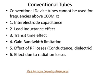
Introduction
Limitations
of
conventional
tubes
at
microwave
frequencies:
Conventional vacuum tube
like
triodes,
tetrodes
and
pentodes
are
less
useful
signal
source
at
the
frequency
above
the
300
MHz.
To
see
whether
or
not
a
conventional
device
works
satisfactory
at
high
frequencies or
microwave
frequencies,
we
consider
a
simple
oscillator
having
LC
tuned
circuit
and
try
to
increase
the
operating
frequency.
For
this
purpose
we
reduce
the
tank
circuit
parameter,
either
L
or
C
(since
τ
=d/v0).
For
high
frequency
or
microwave
frequency
the
device
parameters
like
the
inter
electrode
capacitance
and
lead
inductance
takes
the
dominant
part
in the
circuit
and
affect
the
operation
of
the
oscillator.
35
35
Introduction
There
are
following
reasons
for
that
conventional
tube
cannot
be
used
for
microwave
frequency
or
high
frequency.
1.
Inter
electrode
capacitance
and
lead
inductance
effect.
2.
Transit
time
effect.
3.
Gain-Bandwidth
product
limitation.
4.
RF
losses.
5.
Radiation
losses.
36
36
1.
Inter
electrode Capacitance
and Lead
Inductance
Effect:
The
inter
electrode
capacitances and
lead
inductances
are
the
order
of
1
to
2
pF
and
15
to
20
mH
respectively.
The
shunt
impedances
due
to
inter
electrode
becomes
very
low
and
series
impedances
due
to
lead
inductance
become
very high
at
the
microwave
or high frequency which
makes
these tube
unstable. Refinements
have
been done
in
the
design
and
fabrication
of
these tubes with the
result that
these tubes,
like
disk
seal
tube,
are
still
used
up
to
the
lower
end
of
microwave
spectrum.
2.
Transit
Time
Effect:
In a
conventional
tube
electrons
emitted
by
the
cathode
take
a
finite
(non-zero)
time
in
reaching
the
anode.
This
interval,
called
the
transit
time, depends on
the
cathode
anode
spacing
and the
static voltage
between
the anode and the.
Transit
time (τ)
=
where
τ is
the transit
time,
d is the
cathode
anode
spacing
and is the
velocity
of electrons.
37
37
3.
Gain-Bandwidth
Product Limitation:
In
ordinary vacuum
tubes the
maximum
gain
is
generally achieved by resonating
the
output
tunes
circuit.
Gain-bandwidth
product
=
Amax
BW
= (gm/
G) (G/C)
Where
gm
is
the
transconductance,
Amax·BW
=
gm/
C
.
It
is
important
to
note
that
the
gain-bandwidth
product
is
independent of
frequency.
As
gm
and C
are
fixed
for
a
particular
tube
or
circuit,
higher
gain
can
be
achieved
only
at
the
applicable
to
resonant
circuit
only.
38
38
In
microwave
device
either
re-entrant
cavities
or
slow-
wave
structures
are
used
to
obtain
a
possible
overall
high
gain
over
a
broad
bandwidth.
4.
RF
Losses:
RF
losses include the skin
effect
losses
and
dielectric
losses.
(a)
Skin
effect
losses:
Due
to
skin
effect,
the
conductor
losses
came
into play
at
higher
frequencies,
at
which the
current
has the
tendency
to
confined
itself
to
a
smaller
cross-section
of
the
conductor
towards
its
outer
surface.
39
39
(b)Dielectric
losses:
At
the
microwave
frequency
or
high
frequency various insulating
materials
like
glass
envelope,
silicon
and
plastic
encapsulations
are
used.
The
losses
occur
due
to
dielectric
materials
is
known
as
dielectric
loss
generally
the
relationship
between
the
power
loss
in
dielectric
and
frequency
is
given by
PL
𝖺
f
So,
if
frequency increases
then
power
loss will
also
increases.
The
effect
of
dielectric
loss
can
reduced
eliminating
the tube
base
and
reducing
the
surface
area
of
the
dielectric
material.
5. Radiation Losses:
At
high
frequency,
when
the
dimensions
of
wire approaches
near
to
the
wavelength
(λ =
c/f).
It
will emit
radiation
called
radiation
losses. Radiation losses
are
increases
with
the
increase
in
frequency.
Radiation loss
can
be reduced
by
proper
shielding
of
the tube
and
its
circuitry.
40
40
K
l
y
s
t
r
on
Klystron
is
the
simplest
vacuum
tube
that
can
be
used
for
amplification
or
generation
(as
an
oscillator)
of
microwave
signal.
The
operation
of
klystron
depends
upon
velocity
modulation
which
leads
to
density
modulation
of
electrons.
Klystron
may
be classified
as
gives
below: 1.
Two
cavity
klystron
amplifier
2.
Multi
cavity
klystron
3.
Reflex
klystron.
41
41
TWO
CAVITY
KLYSTRON
AMPLIFIER
One of
the earlier
form
of
velocity
modulation device
is
the
two
cavity
klystron
amplifier,
represented by
the
schematic of
figure.
It
is
seen
that
high
velocity
electron
beam
is
formed,
focused
and
sent
down
along a glass tube
to
a
collector
electrode,
which
is
at
a
high
positive potential
with respect
to
the
cathode.
As
it is
clear
from
the figure,
a
two
cavity klystron
amplifier
consists
of
a
cathode,
focussing
electrodes,
two
buncher grids
separated
by
a
very
small
distance
forming
a
gap
A
(Input
cavity
or
buncher
cavity), two
catcher
grids with a
small
gap
B
(output or
catcher
cavity)
followed
by
a
collector.
42
42
F
i
g
u
r
e
43
43
Operation
The
input
and
output
are
taken
from
the
tube
is
via
resonant
cavity
with
the
help
of
coupling
loops.
The
region
between buncher
cavity
and
catcher cavity
is
called drift space.
The
first
electrode
(focussing
grid)
controls
the
number
of
electrons
in the
electron
beam
and
serves
to focus
the
beam.
The
velocity
of
electrons
in
the
beam
is
determined
by
the
beam
accelerating potential.
On
leaving
the
region
of
focussing
grid,
the
electrons passes through
the
grids
of buncher
cavity.
The
space
between
the
grids
is
referred
to
as
interaction
space.
When
electrons
travel
through
this
space,
they
are
subjected
to
RF
potential
at
a
frequency
determined
by
the
cavity
resonant
frequency
which
is
nothing
but
the
input
frequency.
44
44
Operation
The
amplitude
of
this
RF
potential
between the
grids is
determined
by
the
amplitude
of
the input
signal
in
case of
an
amplifier
or
by
the
amplitude
of
feedback
signal
from
the
second
cavity
if
used
as an
oscillator.
The
working
of
two
cavity
klystron
amplifier
depends
upon
velocity modulation.
45
45
Velocity
Modulation Consider
a
situation
when
there
is
no
voltage
across
the
gap.
Electrons
passing
through
gap
A
are
unaffected
and
continue
on
to
the
collector
with
the
same
constant
velocities
they
had
before
approaching
the
gap
A.
When RF
signal
to
be amplified
is
used
for
exciting
the
buncher
cavity
thereby
developing
an
alternating
voltage
of
signal
frequency
across
the
gap
A.
The
theory
of velocity modulation
can
be
explain
by
using
the
diagram
known
as
Applegate
diagram
as
shown
in
figure.
At
point
X
on
the
input RF
cycle,
the
alternating
voltage
is
zero
and
electron which
passes
through
gap
A
is
unaffected
by
the
RF
signal
46
46
Let
this
electron
is
called
reference
electron
eR which
travels
with
an
unchanged
velocity
,
where
V
is
the
anode
to
cathode
voltage.
Consider
another
point
Y of the RF
cycle
an
electron passing
the
gap
slightly later
than
the
reference
electron
eR,
called
the
late
electron
eL
is
subjected
to
positive
RF
voltage
so
late
electron
eL
is
accelerated
and
hence
travelling
towards
gap
B
with
an
increased velocity
and this
late
electron
eL tries
to
catch
the
reference
electron
eR.
Similarly,
another
point
Z
of RF
cycle,
an
electron
passing
the
gap
slightly
before
than
the
reference
electron
eR,
called
the early
electron
ee
and
this
early
electron
is
subjected
to
negative
RF
voltage
so
early
electron
ee
is
retarded
and
hence
travelling
towards
gap
B
with
reduced
velocity
and
reference
electron
eR
catches
up
the
early
electron
ee.
47
47
So,
when the
electron pass
through
the buncher
gap
their
velocity
will
be
change according
to
the
input
RF
signal.
This
process
is
known
as
velocity
modulation.
48
48
Applegate
diagram,
the
electrons
gradually
bunch
together
as
they
travel
in
the drift
space. When an
electron
catches
up
with
another
one,
the
electron
will
exchange
energy
with the
slower electron,
giving
it
some
excess
energy
and
they
bunch
together
and
move
on
with
the
average
velocity of the beam. This phenomena
is
very
vital
to
the
operation
of
klystron
tube
as
an
amplifier.
The
pulsating
49
49
s
t
r
e
a
m
o
f
el
e
c
t
r
on
s
passe
s
th
r
oug
h
g
ap
B
and
e
x
ci
t
ed
oscill
a
tion
i
n
the
outpu
t
c
a
vi
t
y
.
Th
e
densit
y
o
f
el
e
c
t
r
o
n
passing the
gap
B
varies cyclically
with time. This
mean
the
electron
beam
contains
an
AC
current
and
variation
in
current
density
(often called current
modulation) enables
the
klystron
to
have
a
significant
gain
and
hence
drift
space
converts
the
velocity
modulation
into
current
modulation.
50
50
Bunching
process
The electrons
gradually
bunch
together
due
to
the
difference
in
velocities
of
the
electrons,
as
they
travel
down
the
drift space.
The variation
in
electron
velocity
in drift space
is known as
velocity
modulation
and the
density of
electrons
in
the
bunches
and
catcher
cavity
gap
varies
cyclically
with
time,
i.e.
become
density
modulated.
According
to
fig.
the
distance
from
buncher
grid
to
the
buncher
location
is
L
and
initially
we
consider
for
electron
B,
51
51
52
52
Output
Power
and
Efficiency
The
electronic
efficiency
of
the
two
cavity
klystron
amplifier
is
defined
as
the
ratio
of
the
output
power
to
the
input
power
Efficiency
‘
’
=
P
0
/P
in
=
P
ac
/P
dc
From
previous
equations,
=
(0.58).
V
2
/V
0
and
the
voltage
V
2
is
equal
to
V
0
,
then
maximum
efficiency
max
=
58%
But
in practice
the
efficiency
is
in
the
range
of
15
to
40%.
53
53
Multi
cavity
Klystron
amplifier
Klystron
amplification, power
output,
and
efficiency can
be
greatly
improved
by
the
addition
of
intermediate
cavities
between
the
input
and
output
cavities
of
the
basic
klystron.
Additional
cavities
serve
to
velocity-modulate
the
electron
beam
and
produce
an
increase
in the
energy
available
at
the
output. Since
all
intermediate cavities
in a
multi
cavity
klystron
operate
in
the
same
manner,
a
representative
three-cavity
klystron
will
be
discussed.
54
54
Multi
cavity
klystron
amplifier
Construction:
A
three-cavity
klystron
is
illustrated
in
figure.
The
entire
drift-tube
assembly,
the
three cavities,
and
the
collector
plate
of
the
three-cavity
klystron
are
operated
at
ground
potential
for
reasons
of
safety.
The electron beam
is
formed
and
accelerated
toward
the
drift
tube
by
a
large
negative
pulse
applied
to
the cathode.
Magnetic
focus
coils
are
placed
around
the
drift
tube
to
keep
the
electrons
in a
tight
beam
and
away
from
the
side
walls of
the tube.
The
focus
of
the
beam
is also
aided
by
the
concave
shape
of
the
cathode
is
high-powered
klystrons.
55
55
Fi
g
u
r
e
56
56
Operation
of
Multi
cavity
Klystron
The output of
any
klystron (regardless
of
the
number of
cavities
used)
is
developed
by
velocity modulation of
the
electron
beam.
The
electrons
that
are
accelerated
by
the
cathode
pulse
are
acted upon
by
RF
fields developed
across
the input
and middle
cavities. Some electrons
are
accelerated,
some
are
decelerated,
and
some
are
unaffected.
Electron
reaction
depends
on
the
amplitude
and polarity of
the
fields
across
the
cavities
when the
electrons
pass the
cavity
gaps.
During the
time
the
electrons
are
travelling
through
the
drift
space
between
the
cavities,
the
accelerated
electrons
overtake
the
decelerated
electrons
to
form
bunches.
As a
result, bunches of electrons arrive
at
the
output
cavity
at
the
proper
instant
during
each
cycle of the
RF
field
and
deliver
energy
to
the
output
cavity.
Only
a
small
degree
of bunching
takes
place
within
the
electron
beam
during
the
interval
of
travel
from
the
input
cavity
to
the middle
cavity.
57
57
The amount of bunching
is
sufficient,
however,
to
cause
oscillations
within
the
middle
cavity
and
to
maintain
a
large
oscillating
voltage
across
the
middle
cavity
gap.
Most
of
the
velocity
modulation
produced
in
the
three-cavity
klystron
is
caused
by the
voltage
across
the
input
gap
of
the middle
cavity.
The high
voltage
across
the
gap
causes
the
bunching
process
to
proceed
rapidly
in the
drift space
between
the middle
cavity
and
the
output
cavity.
The electron bunches
cross
the
gap
of the
output
cavity
when
the
gap
voltage
is
at
maximum
negative.
58
58
Maximum
energy
transfer
from
the
electron beam
to
the
output
cavity
occurs
under
these
conditions.
The
energy
given
up
by
the
electrons
is
the
kinetic
energy
that
was
originally
absorbed
from
the
cathode
pulse.
Klystron
amplifiers
have
been built
with
as
many
as
five intermediate cavities
in
addition
to
the
input
and
output
cavities.
The
effect
of
the
intermediate
cavities
is
to
improve
the
electron
bunching
process
which
improves
amplifier
gain.
The
overall
efficiency of
the
tube is
also
improved
to
a
lesser
extent.
59
59
Reflex
Klystron
Reflex
klystron
is
low
power,
low efficiency
microwave
oscillator.
Reflex
klystron
is a
single
cavity
variable
frequency
microwave
generator.
This
is
most
widely
used
in
application
where
variable
frequency
is
desired
like
radar
receiver
and
microwave
receivers. Construction:
Reflex
klystron
consists
of
an
electron
gun similar
to
that
of multi
cavity klystron,
a
filament
surrounded
by
a
cathode
and
a
focussing
electrode
at
the
cathode
as
shown
in
figure.
The
reflex
klystron
contains
a
repeller
which
is
at
a
high
negative
potential.
60
60
Reflex
Klystron
The
suitable
formed
electron
beam
is
accelerated
towards
the
cavity,
where
a
high
positive
voltage
applied
to
it.
This
acts as anode and
known
as
anode
cavity.
After
passing
the
gap
in
cavity electrons
travel towards
repeller
which is
at
high
negative
potential.
The electrons
are
repelled back
from midway
of
the
repeller
space
by
the
repeller
electrode
towards
the
anode.
If
conditions
are
properly adjusted,
then
the
returning
electrons
give
more
energy
to
the
gap
than
they
took
from
it on
forward
journey,
thus
leads
to
sustained
oscillations.
61
61
62
62
Where,
t
0
= time
for
electron
entering
cavity
gap
at
z
= 0
t
1
=
time
for
same
electron
leaving
cavity
gap
at
z
=
d
t
2
= time
for
same
electron returned by
retarding
field
z=d
and
collected
on walls
of
cavity.
Operation
-
The electron beam injected
from
the cathode
is
first
velocity
modulated by
the
beam
voltage.
Some electrons
are
accelerated
and
leave
the
resonator
at
an
increased
velocity
than
those
with
uncharged
velocity.
Some
retarded
electrons
enter
the
repeller
region
with less
velocity.
Then
the
electrons,
which
are
leaving
the
resonator,
will
need
different
time
to
return
due
to
change
in
velocity.
As a
result returning
electrons
group
together
in
bunches. It
is
seen
that
earlier
electrons
take
more
time
to
return
to
the
gap
than
later electrons
and
so
the
conditions
are
right
for
bunching
to
take
place.
63
63
On
their
return
journey
the
bunched
electrons
pass
through
the
gap
during
the
retarding
phase of
the
alternating
field
and
give
up
their
Kinetic
energy
to
the
e.m. energy of
the
field
in
the
cavity.
Or
as the
electron
bunches pass
through
resonator,
they
interact
with
voltage at
resonator
grids. If
the
bunches pass
the
grid
at
such time
that the electrons
are
slowed down by
the
voltage,
energy will be
delivered
to
the
resonator
and
electrons
will
oscillate.
The
electrons
finally
collected by
the
walls of
the
cavity
or
other
grounded
metal
parts
of
the
tube.
64
64
Applegate
diagram
65
65
Operation
through
Applegate
diagram
-
The
early
electron
e
e
that
passes
through
the
gap,
before
the
reference
electron
e
R
,
experiences
a
maximum
+ve
voltage
across
the
gap
and
the
electron
is
accelerated,
it
moves
with
greater
velocity
and
penetrates
deep
into
repeller
space.
The
return
time
for
electron
e
e
is
greater
as
the
depth
of
penetration
into
the
repeller space
is
more.
Hence
e
e
and e
R
appear
at
the
gap
fpr
second
time
at
the
same
instant.
66
66
The
late
electron
e
L
that
passes
the
gap,
later
than
reference
electron
e
R
,
experiences
a
maximum
–ve
voltage
and
moves
with
a
retarding
velocity.
The
return
time
is
shorter
as
the
penetration
into
repeller
space
is
less
and
catches
up
with
reference
electron
e
R
and
earlier
electron
e
e
and
forming
a
bunch.
Bunches
return
back
and
pass
through
the
gap
during
the
retarding
phase
of
the
alternating
field
and
give
up
their
maximum
energy
to
the
e.m. energy of
the
field
in the
cavity
to
sustained
oscillations.
67
67
Travelling
wave
tube
Travelling
wave
tube
has
been designed
for
frequencies
as
low
as
300
MHz and
high
as
50
GHz.
The
wide
bandwidth
and
low-
noise
characteristics
makes
the
TWT
ideal
for
used
as
an
amplifier in
microwave
equipment.
For
broadband application,
such
as
satellite,
radar
transmitter,
the
TWT
are
almost
exclusively
used. If
we compare
the
basic
operating
principles
of
TWT
and
klystron,
in
TWT,
the
microwave
circuit
is
non-resonant
and
the
wave
propagates
with
same
speed
as
the
electrons
in
the beam.
The
initial
effect
on
the
beam
is a
small
amount of
velocity modulation caused
by
the
weak electric field
associated
with
the
travelling
wave.
Just
as
in
the
klystron
this
velocity
modulation
later
translates to
current
modulation,
which
then
induces
on
RF
current
in
the
circuit,
causing
amplification.
68
68
69
69
Operation
The
applied RF
signal
propagates
around
the turns
of
the
helix,
and it
produces
an
electric field
at
the
centre
of
the
helix. The
axial
electric field
propagates
with
velocity of
light
multiplied
by
the
ratio
of
the
helix
pitch
to
helix
circumference.
When the
electrons
enter
the
helix
tube,
an
interaction
takes
place
between
the
moving
axial
electric
field
and
the
moving
electrons.
The
interaction
takes
place
between
them
in
such
a
way
that
on
an
average
the
electron
beam
delivers
or
transfer
energy
to
the RF
wave
on
the
helix. This
interaction
causes
the
signal
wave
grows
amplified and
becomes
larger.
70
70
Velocity
Modulation
-
When
the
axial
field
is
zero,
electron
velocity
is
unaffected.
This happens
at
the
point
of node of
the
axial
electric field.
Those electrons entering
the
helix,
when the
axial
field
is
positive
antinode,
at
the
accelerating
field
are
accelerated.
At
a
later
point
where
the
axial
RF
field
is
–ve
antinode,
retarding
field,
the
electrons
are
decelerated.
The
electrons
get
velocity
modulated.
As the
electrons
travel
further
along the
helix, bunching
of
electrons
occur
at
the
end
which
shifts
the
phase
of
/2.
Magnet
produces
axial
magnetic
field
prevents
spreading
of
electron
beam
as
it
travels
down
the
tube.
71
71
Slow
Wave
Structures
(SWS)
SWSs
are
special
circuits
which
are
used
in
microwave
tubes
to
reduce
the
velocity of
wave
in a
certain
direction
so
that
the
electron
beam
and
the
single
wave
can
interact.
The phase velocity of
a
wave
in
ordinary
waveguide
is
greater
than the
velocity of
light
in a
vacuum.
Since the electron beam
can
be
accelerated
only
to
velocities
that
are
about a
fraction
of
the
velocity of light, thus
the
electron
beam
must
keep
in
step
with the
microwave
signal
and a
slow
wave
structure
must
be
incorporated
in the
microwave
devices.
By
which electron beam
and
signal
wave
are travelling
with
nearly
the
same velocity
and
valuable
interaction
takes
place.
72
72
Slow
Wave
Structures
(SWS)
As the
operating
frequency
is
increased,
both
the
inductance
and
capacitance
of
the
resonant circuit must
be decreased
in
order
to
maintain
resonance
at
operating
frequency.
Because
the
gain
bandwidth
product
is
limited
by
the
resonant circuit,
the
ordinary resonator
cannot
generate
a
large
output.
Several
non-resonant
periodic
circuits
or
slow
wave
structures
are
designed
for
producing
large gain
over
a
wide
bandwidth
73
73
74
74
Convection
Current
The
convection current
induced in the
electron beam
by
the
axial electronic
field
and the
microwave
axial
field
produced
by
the
beam
must
first
be developed?
When the
space
charge
effect
is
considered
the
electron
velocity,
charge
density,
current
density
and
axial
electric
field
will
perturbrate
about
their
average
DC
values.
The
schematic
diagram
and
simplified
circuit
of
helix
TWT
are
shown
below
75
75
76
76
The electrons
entering
the
retarding
field
are
decelerated
and
those
in
the
accelerating
field
are
accelerated.
They
begin
forming
a
bunch
centred
about those
electrons
that enter
the
helix
during
the
zero
fields
77
77
Since
the
dc
velocity of
the
electrons
is
slightly
greater
than the
axial
wave
velocity,
more
electrons
in
the
retarding
field
than in the
accelerating
field,
and a
great
amount
of energy
is
transferred
from
the
beam
to
the electromagnetic field. The
microwave
signal
voltage
is
amplified
by
the
amplified
field
The bunch
continues
to
become more compact,
and a
larger amplification
of
the
signal
voltage occurs at
the end
of
the
helix. The
magnet
produces
an
axial
magnetic field
to prevent
spreading
the
electron
beam
as
it
travels
down
the tube.
78
78
An
attenuator
placed
near
the
centre
of
the
helix
reduces
all
the
waves
travelling
along
the
helix
to
nearly
zero
so
that
the
reflected
waves
from
the
mismatched
loads
can
be
prevented
from
reaching
the input and
causing oscillation. The
bunched electrons
emerging
from
the
attenuator
induce a
new
electric
field
with
the
same
frequency.
This
field
in
turn
induces
a
new amplified
microwave
signal
on
the
helix. The magnitude
of
the
velocity
fluctuation
of
the
electron
beam
is
directly
proportional
to
the magnitude
of
the
axial
electric
field
79
79
C
r
o
s
s
-
C
o
u
p
l
e
d
T
u
b
e
s
(
M
a
g
n
e
t
r
o
n
O
s
c
i
l
l
a
t
o
r
)
80
80
Mechanism
of
oscillations
in
Magnetron
-
The
magnetron
requires
an
external
magnetic field
with
flux lines
parallel
to
the
axis
of
cathode.
This field
is
provided by
a
permanent magnet
or
electromagnet.
The dc
magnetic
field
is
normal
to
the
dc electric
field
between
the
cathode
and anode.
Because
of
the
cross-field
between
the
cathode
and
anode,
the
electrons
emitted
from
the
cathode
are affected
by
the
cross-field
to move
in
curved
paths.
If
the
dc
magnetic
field
is
strong
enough,
the
electrons
will
not
arrive
in
the anode
but
return
back
to
the
cathode.
81
81
82
82
Operation-
From
fig
(b).
1.
Path ‘a’
- If there
is no
magnetic
field
present;
the
electron would
be
drawn directly
towards the
anode
in
accordance with
path
‘a’.
2.
Path
‘b’
- As
the
electron
travels
with
a
velocity
the
axial
magnetic field exerts
a
force
on
it.
When the
magnetic
field is
weak
the
electron
path
is
deflected
as
path
‘b’.
3.
Path ‘c’
-
However,
when
the
intensity
of the
magnetic
field
is sufficiently
great,
the electrons
are
turned
back towards the
cathode
without
ever
reaching
the
anode
accordance
with
path
‘c’.
4.
path
‘d’
- The magnetic
field
which
is
just
able to
return
the
electrons
back
to
the
cathode before reaching the anode,
is
termed
the
cut-off
field
as
shown
in
path
‘d’.
Thus
when the magnetic
field
exceeds the
cut-off
value,
then
in
the
absence
of
oscillations
all
the
emitted
electrons
return
to
the
cathode
and
the
plate
current
is
zero.
83
83
-Mode
Oscillations
Let
the
cavity
magnetron
has
8
cavities,
by
which
it
supports
varieties
of
modes
depending
upon
the
phase
difference
between
fields
in
two
adjacent
cavities.
Boundary
conditions
are
satisfied
when
total
phase shift
around
the
eight
cavities
is
multiplied
by
2
radians.
However,
the
most
important
mode
for
magnetron operation
is
one
where
in the
phase shift between
the
fields
of
adjacent
cavities
is
radians.
This
is
known
as
-Mode
.
84
84
Microwave
Solid
State
Devices
Introduction
•
Special
electronics
effects
encountered
at
microwave
frequencies
severely
limit the
usefulness
of
transistors
in
most
circuit
applications.
•
Using
vacuum
tubes
for
low
power
applications
become
impractical.
•
Need
for
small
sized
microwave
devices
has
caused
extensive
research
in
this
area
•
This
research
has
produced
solid-state
devices
with
higher
and
higher
frequency
ranges.
•
The
new
solid
state
microwave
devices
are
predominantly
active,
two
terminal
diodes,
such as
tunnel
diodes,
varactors,
transferred-electron
devices,
and
avalanche
transit-time
diodes
TRANSFERRED
ELECTRON
DEVICES.
⦿
Transferred
electron
devices
(TED’s)
are
bulk
semiconductor
devices
having
no junction.
⦿
TED’s
are
fabricated
from
compound
semiconductor
such
as
GaAs
(gallium
arsenide),
⦿
TED’s
operate
with
hot electrons
whose
energy
is
very
much
greater
than the
thermal
energy.
⦿
the
current
in the
specimen
become
a
fluctuating function of
time.
⦿
Then
negative
resistance
will
manifest
itself
under certain
conditions.
Oscillations
will
occur
if the GaAs
specimen
is
connected
to
a
suitable
tuned
circuit.
⦿
It
is
seen
that
the
voltage
across
the GaAs
is
very
high
and
electron
velocity
is
also
high,
86
86
TWO
VALLEY
THEORY
(RWH
THEORY)
the
two-valley
model,
however,
there
are
two
regions
in
the
conduction
band
in which
charge carriers
(electrons)
can
exist.
These regions
are
called
valleys
and
are
designated
the
upper
valley
and
lower
valley.
According
to
the
RWH
theory,
electrons
in
the
lower valley
have
low
effective
mass
(0.068)
and
consequently
a
high
mobility
(8000
cm2/V-s).
In the
upper
valley,
which is
separated
from
lower
valley
by
potential
of
0.36
eV,
electrons
have
a much
higher
effective
mass
(1.2)
and
lower
mobility (180
cm2/V-
s)
than in the
lower
valley.
Basic
mechanism
involved
in the
operation of
bulk
n-type GaAs
devices
is
the
transfer
of
electrons
from
lower
conduction
valley
to
the
upper
conduction
valley.
Electron density
thus in
lower valley
and
upper
valley
remain
the
same
under
equilibrium
conduction.
87
87
Two
valley
model.
88
88
T
w
o
v
a
l
l
e
y
m
o
d
e
l
.
89
89
When
E
<
El
When
the
applied
electric
field
is
lower
than
the
electric
field
of the
lower
valley
(E
< E
l
),
then
electrons
will
occupy
states
in
the
lower
valley
Thus
the
material
is in
the
highest
average
velocity
state
(electron
in
lower
valley
has
high
mobility)
and
drift
velocity
increases
linearly
with
increasing
potential.
Thus
increasing
the
current
density
J
and
hence
positive
differential
resistance
(ohmic
region).
RWH
theory
is
based
on
population
inversion
principle.
When
El
<
E
< Eu
As
the
applied
field
is
increased
(2–4
kV/cm)
higher
than
that
of
the
lower
valley
and
lower
than
that
of
the
upper
valley
(E
l
<
E <
E
u
),
electrons
will
gain
energy
from
it
and
move
upward
to
upper
valley
As
the
electrons
transfer
to
the
upper
valley,
their
mobility
decreases
and
the
effective
mass
is
increased
thus
decreasing
the
current
density
J
and
hence
negative
differential
resistivity.
Transfer
of
electron
densities.
90
90
Characteristics
of Gunn Diode
91
91
Construction
of
Gunn
Diode
92
92
Equivalent
Circuit
of
Gunn
Diode
D
o
m
a
i
n
M
o
d
e
:
93
93
Disadvantages
of
Gunn Diode
Gunn
dio
de
is
v
e
r
y
mu
c
h
t
e
m
p
e
r
a
tu
r
e
dep
e
nde
n
t
i
.
e
.
,
a
frequency
shift of 0.5
to
3
MHz
per
°
C.
By
proper
design
this
frequency
shift
can
be
reduced
to
50
kHz
for
a
range
of
-
40
°
C
to
70
°
C.
Other
disadvantages
of
Gunn
diode
is,
the
power
output
of
the
Gunn
diode
is
limited
by
difficulty
of
heat
dissipation
from
the
small
chip.
Gunn
diode
is
very
much
temperature
dependent.
94
94
Applications
of
Gunn
Diode
95
95
Gunn
diode
can
be used
as an
amplifier
and as an
oscillator.
The
applications
of
Gunn
diode
are
1.
In
broadband
linear
amplifier.
2.
In
radar
transmitters.
3.
Used
in
transponders
for
air
traffic control.
4.
In
fast
combinational
and
sequential
logic
circuit.
5.
In
low
and
medium
power
oscillators
in
microwave
receivers.
Comparison
Between
Microwave
Transistors
and
TED’s
Microwave
transistors
1
.
Ope
r
at
e
wi
t
h
j
u
nctio
n
o
r
g
at
es.
2.Fabricated
from
elemental
semiconductors
such
as
Si
or
Ge.
3.Operate
with
warm
electrons
whose
energy
is
not
much
greater
than
their
thermal
energy (0.026
eV
at
room
temperature).
TED’s
Operate
with
bulk
devices
having
no
junctions
and
gates.
Fabricated
from
compound
GaAs,
CdTe
or
InP.
Operate
with
hot
electrons
whose
energy
is
very
much
greater
than
th
e
thermal
ene
r
g
y
96
96
A
V
A
L
A
N
C
H
E
T
R
A
N
S
I
T
T
I
M
E
D
E
V
I
C
E
S
In 1958,
Read
at
Bell
Telephone
Laboratories
proposed that
the
delay
between
voltage
and
current
in
an
avalanche,
together
with
transit
time
through
the
material, could
make
a
microwave
diode
exhibit
negative
resistance
such
devices
are
called
Avalanche
transit
time
devices.
The
prominent members
of
this
family
include the
IMPATT
and
TRA
PA
T
T
di
o
d
e
.
1.
IMPATT
(Impact
Ionization Avalanche
Transit
Time) diode as
the
name
suggests,
utilizes
impact
ionization
for
carrier
generation.
2.
TAPATT
(Trapped
Plasma
Avalanche
Triggered
Transit
Time)
diode
is
derived
from
the
IMPATT
with
some
modifications
in
the
doping
profiles
so
as
to
achieve
higher
pulsed
microwave
powers
at
better
efficiency
values.
97
97
IMPATT
DIODE
The
IMPATT
diode
or
IMPact
Avalanche
Transit
time
diode
is
an
RF
semiconductor
device
that
is
used
for
generating
microwave
radio
frequency signal,
with the
ability
to
operate
at
frequencies
between
about
3
to
100
GHz
or
more,
one
of
the
main
disvantages
is
the
relatively
high
power
capability of the
IMPATT
diode.
IMPATT
Structures
There
is a
variety of
structures that
are
used
for
the
IMPATT
diode
like
p+nin+ or n+pip+
read
evice, p+nn+,
and p+in+
diode,
all
are
variations
of
a
basic pn junction
IMPATT
diode
is
semiconductor
device
which
generate microwave
signal
from
3
to
100
GHz.
In
IMPATT
diode,
negative
resistance
effect
phenomenon
is
taken
i
nt
o
ac
c
ou
n
t
98
98
O
p
e
r
a
t
i
o
n
o
f
I
M
P
A
T
T
A
cross-section
of
p+n
n+
IMPATT
diode
structure
is
shown
in
Fig.
7.47.
Note
that
it
is
a
diode,the
junction
being
between
p+
and
then
n
layer.
An
extremely
high
voltage
gradient
is
applied
in
reverse
bias
to
th
e
I
M
P
A
T
T
r
esulting
di
o
de
,
o
f
th
e
o
r
de
r
o
f
40
0
k
V
/
cm,
in
very
high
eventually
current.
99
99
O
p
e
r
a
t
i
o
n
o
f
I
M
P
A
T
T
Such
a
high
potential
gradient,
back-biasing
the
diode,
causes
a
flow
of
minority
carriers
across
the
junction. If
it is
now assumed
that
oscillations
exist.
Now
we
may
consider
the
effect
of
a
positive
swing
of
the
RF
voltage
superimposed
on
top
of
the
high
DC
voltage
100
100
100
E
q
u
i
v
a
l
e
n
t
C
i
r
c
u
i
t
o
f
I
M
P
A
T
T
A
simplified
equivalent
circuit
for
IMPATT
diode
chip is
shown
in
Fig.
Typically
negative
resistance varies
between
-0.7
Ω
and
-2
Ω,
and
capacitance
ranges
from
0.2
to
0.6
pF.
where
Rd =
Diode
negative
resistance consisting
of
the series lead
resistance
Rs and the
negative
resistance
- Rj
due
to
impact
avalanche process.
Cj=
Junction
capacitance.
Lp=
Package
lead
inductance.
Cp=
Package
lead
capacitance.
101
101
101
A
d
v
a
n
t
a
g
e
s
o
f
I
M
P
A
T
T
D
i
o
d
e
102
102
102
IM
PA
T
T
di
o
de
s
a
r
e
a
t
p
r
es
e
n
t
t
h
e
mo
s
t
p
o
w
er
f
u
l
so
l
id
-
s
tat
e
mic
r
o
w
a
v
e
p
o
w
er
sou
r
c
e
s.
Som
e
o
f
the
maj
o
r
ad
v
a
nt
a
g
es
of
IMPATT
diode
1
.
High
er
ope
r
a
ting
r
an
g
e
a
r
e
o
b
t
ain
(
u
p
t
o
100
a
r
e
:
GHz
)
.
2.
Above
about
20
GHz,
the
IMPATT
diode
produces
a
higher
CW
power
output
per
unit
than
any
other
semiconductor
device.
High
er
ope
r
a
ting
r
an
g
e
(u
p
t
o
1
0
0
GHz)
c
an
b
e
o
b
t
ained
f
r
om
IMPATT
diode.
D
i
s
a
d
v
a
n
t
a
g
e
o
f
I
M
P
A
T
T
D
i
o
d
e
103
103
103
The
major
disadvantages
of
IMPATT
diode
are:
1.
Since
DC power
is
drawn
due
to
induced
electron
current
in
the
external circuit,
IMPATT
diode
has
low efficiency
(RF
power
o
u
tput
/
D
C
input
p
o
w
er
)
.
2.
Tend
to
be
noisy
due primarily
to
the
avalanche process
and
to
the
high
level
of
operating
current.
A
typical
noise
figure
is
30
dB
which
is
w
o
r
s
e
than
3
.
T
unin
g
is
di
fficul
t
as
that
of
c
ompa
r
e
to
Gunn
Gunn
diod
e.
di
o
d
e
.
4.
To
run
an
IMPATT
diode,
a
relatively
high
voltage
is
required.
A
p
p
l
i
c
a
t
i
o
n
s
o
f
I
M
P
A
T
T
D
i
o
d
e
IMPATT
diodes
are
used
as
microwave
oscillators
such
as:
1.
Used
in
final
power
stage
of
solid
state
microwave
transmitter
for
communication
purpose.
2.
Used
in
transmitter
of
TV
system.
3.
Used
in
FDM/TDM
system.
4.
Used
in
microwave
source
in
laboratory
for
measurement
purpose.
Photograph
of
a
IMPATT
diode
is
shown
in
Fig.
7.52.
104
104
104
C
o
m
p
a
r
i
s
o
n
b
e
t
w
e
e
n
G
u
n
n
d
i
o
d
e
a
n
d
I
m
p
a
t
t
d
i
o
d
e
105
105
105
Microwave and radar engineering involve the study of electromagnetic radiation with wavelengths ranging from one meter to one millimeter and frequencies between 300 MHz and 300 GHz. This form of technology plays a crucial role in communication systems due to its advantages such as large bandwidth, better directivity, and the ability to use small-sized antennas.

Download Presentation

Please find below an Image/Link to download the presentation.
The content on the website is provided AS IS for your information and personal use only. It may not be sold, licensed, or shared on other websites without obtaining consent from the author. Download presentation by click this link. If you encounter any issues during the download, it is possible that the publisher has removed the file from their server.
E N D
Presentation Transcript
MICROWAVE & RADAR ENGINEERING
Introduction Microwaves are with wavelengths ranging from about one meter to one millimeter; with frequencies between 300 MHz (1 m) and 300 GHz (1 mm). a form of electromagnetic radiation A more common definition in radio engineering is the range between 1 and 100 GHz (wavelengthsbetween 0.3 m and 3 mm). Microwaves include the entire SHF band (3 to 30 GHz, or 10 to 1 cm) at minimum. Frequencies in the microwave range are often referred to by their IEEE radar band designations: L,S, C, X, Ku, K, or KabanD. 2
prefix micro-in microwave is not meant to suggest a wavelength in the micrometerrange. Rather, it indicates that microwaves are "small" (having shorter wavelengths), compared to the radio waves used prior to microwave technology. The boundaries between far microwaves, and ultra-high-frequency radio waves are fairly arbitrary and are used variously between different fields of study. Microwaves travel by line-of-sight; unlike lower frequency radio waves they do not diffract around hills, follow the earth's surface as ground waves, or reflect from the ionosphere. so terrestrial microwave communication links are limited by the visual horizon to about 40 miles infrared, terahertz radiation, 3
MICROWAVE BANDS Microwavefrequency bands Designation Frequency range Wavelength range Lband 1 to 2 GHz 15 cm to 30 cm Sband 2 to 4 GHz 7.5cm to 15 cm Cband 4 to 8 GHz 3.75cm to 7.5 cm X band 8 to 12GHz 25 mm to 37.5 mm 5
Kuband 12 to 18 GHz 16.7mm to 25 mm K band 18 to 26.5 GHz 11.3mm to 16.7 mm Kaband 26.5to40 GHz 5.0 mm to 11.3 mm Qband 33 to 50 GHz 6.0mm to 9.0 mm Uband 40 to 60 GHz 5.0mm to 7.5 mm 6
ADVANTAGES OF MICROWAVES Large Bandwidth: The Bandwidth of Microwaves is larger than the common low frequency radio waves. Thus more information can be transmitted using Microwaves. It is very good advantage, because of this, Microwaves are used for Point to Point Communications. Better Directivity: At Microwave Frequencies, there are better directive properties. This is due to the relation that As Frequency Increases, Wavelength decreases and as Wavelength decreases Directivity Increases and Beam width decreases. So it is easier to design and fabricate high gain antenna in Microwaves 7
Small Size Antenna: Microwaves allows to decrease the size of antenna. The antenna size can be smaller as the size of antenna is inversely proportional to the transmitted frequency. Thus in Microwaves, we have waves of much higher frequencies and hence the higher the frequency, the smallerthe size of antenna. Low Power Consumption: The power required to transmit a high frequency signal is lesser than the power required in transmission of low frequency signals. As Microwaves have high frequency thus requires very less power. Effect Of Fading: The effect of fading is minimized by using Line Of Sight propagation Frequencies. While at low frequency signals, the layers around the earth causes fading of the signal technique at Microwave 8
APPLICATIONS OF MICROWAVES There Applications of Microwaves. The great example of Application of Microwavesis 'Microwave Oven' which we uses in our daily life. are many Industrial, Scientific, Medical and Domestic Following are the other main applicationareas of Microwaves: Communication RemoteSensing Heating MedicalScience 9
Communication: Microwave is used in broadcasting and telecommunication transmissions. As described above, they have shorter wavelengths and allows to use smaller antennas. The cellular networks like GSM, also uses Microwave frequencies of communication. Microwaves are also used for transmitting and receiving a signal from earth to satellite and from satellite to earth. Military or Army also makes use of Microwaves communication system. They uses X or Ku band communication. range 1.8 to 1.9 GHz for in t h e i r for their 10
Remote Sensing: Most of you may be familiar with this Application. The most common application of Microwave is its use in RADAR and SONAR. RADAR is used to illuminate an object by using a transmitter and receiver to detect its position and velocity. Radiometry is also one of the RemoteSensing Applications. Heating: You all are familiar with this application. We uses Microwave Oven to bake and cook food. It is very convenient electronic machine which performs the heating task very cleanly and in a very less time. If you Want to know How Does a Microwave Works? then you may wonder that is based on the vibration of electrons present in the Food Particles. That is why Microwave Oven heats the food uniformly without heating the container. 11
Medical Science: Microwave's heating properties are also used in Medical Science. Microwave also have Medical Applications such as it is used in diagnosis and various therapies. There are also some other applications of heating as Drying, Precooking and Moisture Leveling. property of microwave such 12
WAVEGUIDES A hollow metallic tube of the uniform cross section for transmitting electromagnetic waves by successive reflections from the inner walls of the tube is called as a Waveguide. Microwaves propagate through microwave circuits, components and devices, which act as a part of Microwave transmission lines, broadly called as Waveguides. A waveguide is generally preferred in microwave communications. A waveguide is a special form of a transmission line, which is a hollow metal tube. Unlike the transmission line, the waveguide has no center conductor. 13
ADVANTAGES OF WAVEGUIDES Waveguidesare easy to manufacture. They can handle very large power (in kilowatts) Power loss is very negligible in waveguides They offer very low loss ( low value of alpha-attenuation) The microwave energy when travels through the waveguide, experienceslower losses than a coaxial cable. 14
Types of waveguides There are five types of waveguides. They are: Rectangularwaveguide Circularwaveguide Ellipticalwaveguide Singleridged waveguide Doubleridged waveguide 15
TransmissionLines Waveguides SupportsTEM wave Cannotsupport TEM wave Only the frequencies that are greater than cut-off frequency can pass through Allfrequenciescan pass through One conductor transmission Twoconductor transmission Wave travels through reflections from the wallsof waveguide Reflectionsare less It has characteristicimpedance It has wave impedance 17
Propagation of waves is accordingto "Circuittheory" Propagation of waves is accordingto"Field theory" Returnconductor is not required as the body of the waveguide acts as earth It has a return conductor to earth Bandwidth is not limited Bandwidthis limited Waves do not disperse Waves getdispersed 18
Rectangular Waveguides Rectangular waveguides are the one of the earliest type of the transmissionlines. They are used in many applications. A lot of components such as isolators, detectors, attenuators, couplers and slotted lines are available for various standard waveguide bands between 1 GHz to above 220 GHz. A rectangular waveguide supports TM and TE modes but not TEM waves because we cannot define a unique voltage since there is only one conductor in a rectangularwaveguide. The shape of a rectangular waveguide is as shown below. A material with permittivity e and permeability m fills the inside of the conductor. 19
A rectangular waveguide cannot propagate below some certain frequency. This frequency is called the cut-off frequency. Here, we will discuss TM mode rectangular waveguides and TE mode rectangular waveguides separately. 20
Modes of wave guides Waveguide modes Looking at waveguide theory it is possible it calculate there are a number of formats in which an electromagnetic wave can propagate within the waveguide. These different types of waves correspond to the different elements within an electromagneticwave. TE mode: This waveguide mode is dependent upon the transverse electric waves, also sometimes called H waves, characterized by the fact that the electric vector (E) being always perpendicular to the direction of propagation. In TE wave only the E field is purely transverse to the direction of propagation and the magnetic field is not purely transverse i.e.Ez=0,Hz#0 21
TM mode: Transverse magnetic waves, also called E waves are characterised by the fact that the magnetic vector (H vector) is always perpendicular to the direction of propagation. In TE wave only the H field is purely transverse to the direction of propagationand the Electric field is not purely transverse i.e.Ez#0,Hz=0 TEM mode: The Transverse electromagnetic wave cannot be propagated within a waveguide, but is included for completeness. It is the mode that is commonly used within coaxial and open wire feeders. The TEM wave is characterised by the fact that both the electric vector (E vector) and the magnetic vector (H vector) are perpendicular to the direction of propagation. In this neither electric nor magnetic fields are purely transverse to the direction of propagation.i.e. Ez#0, Hz#0 22
Modes The electromagnetic wave inside a waveguide can have an infinite number of patternswhich are called modes. The electric field cannot have a component parallel to the surface i.e. the electric field must always be perpendicular to the surface at the conductor. The magnetic field on the other hand always parallel to the surface of the conductor and cannot have a component perpendicular to it at the surface. 23
We have seen that in a parallel plate waveguide, a TEM mode for which both the electric perpendicular to the direction of propagation, exists. This, however is not true of rectangular wave guide, or for that matter for any hollow conductor wave guide without an inner conductor.We know that lines of H are closed loops. Since there is no z component of the magnetic field, such loops must lie in the x-y plane. However, a loop in the x-y plane, according to Ampere slaw,implies an axial current. If there is no inner conductor, there cannot be a real current. The only other possibility then is a displacementcurrent. and magnetic fields are 24
However, an axial displacement current requires an axial component of the electric field, which is zero for the TEM mode. Thus TEM mode cannot exist in a hollow conductor. (for the parallel plate waveguides, this restriction does not apply as the field lines close at infinity.) 25
Guided Wavelength (g) Guided Wavelength ( g): It is defined as the distance travelled by the wave in order to undergo a phase shift of 2 radians. It is related to phase constant by the relation g=2 / the wavelength in the waveguide is different fromthe wavelengthin free space. Guide wavelength is related to free space wavelength 0 and cut-off wavelength c by 1/ g2=1/ 02-1/ c2 The above equation is true for any mode in a waveguideof any cross section 26
Phase Velocity(vp) Phase Velocity(vp): Wave propagates in the waveguide when guide wavelength gis grater than the free space wavelength 0. In a waveguide, vp= gf where vp is the phase velocity. But the speed of light is equal to product of 0and f. This vp is greater then the speed of light since g> 0. The wavelength in the guide is the length of the cycle and vp represents the velocityof the phase. It is defined as the rate at which the wave changes its phase in terms of the guide wavelength. Vp= / Vp=c/[1-( 0/ c)2]1/2 27
Degenerate Modes Degenerate Modes Two or more modes having the same cut-off frequency are called Degenerate modes For a rectangularwaveguide TEmn/TMmnmodes for which both m#0,n#0 will always be degenerate modes. 28
Matched load: Matched Load is a device used to terminate a transmission line or waveguide so that all the energy from the signal source will be absorbed. 29
CIRCUALTORS AND ISOLATORS Both microwave circulators and isolators are non reciprocal transmission devices that use the property of Faraday rotation in the ferrite material. A non reciprocal phase shifter consists of thin slab of ferrite placed in a rectangular waveguide at a point where the dc magnetic field of the incident wave mode is circularly polarized. When a piece of ferrite is affected by a dc magnetic field the ferrite exhibits Faraday rotation. It does so because the ferrite is nonlinear material and its permeability is an asymmetric tensor. 30
MICROWAVECIRCULATORS A microwave circulator is a multiport waveguide junction in which the wave can flow only from the nth port to the (n + I)th port in one direction Although there is no restriction on the number of ports, the four-port microwave circulator is the most common. One type of four-port microwave circulator is a combination of two 3-dB side hole directional couplers and a rectangularwaveguide with two non reciprocal phase shifters. 31
ISOLATOR An isolator is a nonreciprocal transmission device that is used to isolate one component from reflections of other components in the transmission line. An ideal isolator completely absorbs the power for propagation in one direction and provides lossless transmission in the opposite direction. Thus the isolator is usually called uniline. 33
Introduction Limitations of conventional tubes at microwave frequencies: Conventional vacuum tube like triodes, tetrodes and pentodes are less useful signal source at the frequency above the 300 MHz. To see whether or not a conventional device works satisfactory at high frequencies or microwave frequencies, we consider a simple oscillator having LC tuned circuit and try to increase the operating frequency. For this purpose we reduce the tank circuit parameter, either L or C (since =d/v0). For high frequency or microwave frequency the device parameters like the inter electrode capacitance and lead inductance takes the dominant part in the circuit and affect the operation of the oscillator. 35
Introduction There are following reasons for that conventional tube cannot be used for microwave frequency or high frequency. 1. Inter electrode capacitanceand lead inductanceeffect. 2. Transit time effect. 3. Gain-Bandwidth product limitation. 4. RFlosses. 5. Radiationlosses. 36
1.Inter electrode Capacitance and Lead Inductance Effect: The inter electrode capacitances and lead inductances are the order of 1 to 2 pF and 15 to 20 mH respectively. The shunt impedances due to inter electrode becomes very low and series impedances due to lead inductance become very high at the microwave or high frequency which makes these tube unstable. Refinements have been done in the design and fabrication of these tubes with the result that these tubes, like disk seal tube, are still used up to the lower end of microwave spectrum. 2.Transit Time Effect: In a conventional tube electrons emitted by the cathode take a finite (non-zero) time in reaching the anode. This interval, called the transit time, depends on the cathode anode spacing and the static voltage between the anode and the. Transit time ( ) = where is the transit time, d is the cathode anode spacing and is the velocity of electrons. 37
3. Gain-Bandwidth Product Limitation: In ordinary vacuum tubes the maximum gain is generally achieved by resonating the output tunes circuit. Gain-bandwidth product = Amax BW = (gm/ G) (G/C) Where gm is the transconductance, Amax BW= gm/ C . It is important to note that the gain-bandwidth product is independent of frequency. As gm and C are fixed for a particular tube or circuit, higher gain can be achieved only at the applicable to resonant circuit only. 38
In microwave device either re-entrant cavities or slow- wave structures are used to obtain a possible overall high gain over a broad bandwidth. 4. RF Losses: RF losses include the skin effect losses and dielectric losses. (a) Skin effect losses: Due to skin effect, the conductor losses came into play at higher frequencies, at which the current has the tendency to confined itself to a smaller cross-section of the conductor towards its outer surface. 39
(b)Dielectric losses: At the microwave frequency or high frequency various insulating materials like glass envelope, silicon and plastic encapsulations are used. The losses occur due to dielectric materials is known as dielectric loss generally the relationship between the power loss in dielectric and frequency is given by PL ? f So, if frequency increases then power loss will also increases. The effect of dielectric loss can reduced eliminating the tube base and reducing the surface area of the dielectricmaterial. 5. Radiation Losses: At high frequency, when the dimensions of wire approaches near to the wavelength ( = c/f). It will emit radiation called radiation losses. Radiation losses are increases with the increase in frequency. Radiation loss can be reduced by proper shielding of the tube and its circuitry. 40
Klystron Klystron is the simplest vacuum tube that can be used for amplification or generation (as an oscillator) of microwave signal. The operation of klystron depends upon velocity modulation which leads to density modulation of electrons. Klystron may be classified as gives below: 1. Two cavity klystron amplifier 2. Multi cavity klystron3. Reflex klystron. 41
TWO CAVITY KLYSTRON AMPLIFIER One of the earlier form of velocity modulation device is the two cavity klystron amplifier, represented by the schematic of figure. It is seen that high velocity electron beam is formed, focused and sent down along a glass tube to a collector electrode, which is at a high positive potential with respect to the cathode. As it is clear from the figure, a two cavity klystron amplifier consists of a cathode, focussing electrodes, two buncher grids separated by a very small distance forming a gap A (Input cavity or buncher cavity), two catcher grids with a small gap B (output or catcher cavity)followed by a collector. 42
Figure 43
Operation The input and output are taken from the tube is via resonant cavity with the help of coupling loops. The region between buncher cavity and catcher cavity is called drift space. The first electrode (focussing grid) controls the number of electrons in the electron beam and serves to focus the beam. The velocity of electrons in the beam is determined by the beam accelerating potential. On leaving the region of focussing grid, the electrons passes through the grids of buncher cavity. The space between the grids is referred to as interaction space. When electrons travel through this space, they are subjected to RF potential at a frequency determined by the cavity resonant frequency which is nothing but the input frequency. 44
Operation The amplitude of this RF potential between the grids is determined by the amplitude of the input signal in case of an amplifier or by the amplitude of feedback signal from the second cavity if used as an oscillator. The working of two cavity klystronamplifier depends upon velocity modulation. 45
Velocity Modulation Consider a situation when there is no voltage across the gap. Electrons passing through gap A are unaffected and continue on to the collector with the same constant velocities they had before approaching the gap A. When RF signal to be amplified is used for exciting the buncher cavity thereby developing an alternating voltage of signal frequency across the gap A. The theory of velocity modulation can be explain by using the diagram known as Applegate diagram as shown in figure. At point X on the input RF cycle, the alternating voltage is zero and electron which passes through gap A is unaffected by the RF signal 46
Let this electron is called reference electron eR which travels with an unchanged velocity , to cathode voltage. Consider another point Y of the RF cycle an electron passing the gap slightly later than the reference electron eR, called the late electron eL is subjected to positive RF voltage so late electron eL is accelerated and hence travelling towards gap B with an increased velocity and this late electron eL tries to catch the reference electron eR. Similarly, another point Z of RF cycle, an electron passing the gap slightly before than the reference electron eR, called the early electron ee and this early electron is subjected to negative RF voltage so early electron ee is retarded and hence travelling towards gap B with reduced velocity and reference electroneR catches up the early electronee. where V is the anode 47
So, when the electron pass through the buncher gap their velocity will be change according to the input RF signal.This process is known as velocity modulation. 48
Applegate diagram, the electrons gradually bunch together as they travel in the drift space. When an electron catches up with another one, the electron will exchange energy with the slower electron, giving it some excess energy and they bunch together and move on with the average velocity of the beam. This phenomena is very vital to the operation of klystron tube as an amplifier. The pulsating stream of electrons passes through gap B and excited oscillation in the output cavity. The density of electron passing the gap B varies cyclically with time. This mean the electron beam contains an AC current and variation in current density (often called current modulation) enables the klystron to have a significant gain and hence drift space converts the velocitymodulationinto current modulation. 49


")
")


Dielectric losses: At the microwave frequency or high")