Microwave Diodes and Transfer Electron Devices in Radar Systems

22/8/14
S
u
b
j
e
c
t
N
a
m
e
:
M
i
c
r
o
w
a
v
e
a
n
d
R
a
d
a
r
S
u
b
j
e
c
t
C
o
d
e
:
1
0
E
C
5
4
P
r
e
p
a
r
e
d
B
y
:
L
a
k
s
h
m
i
C
R
,
D
h
a
r
a
n
i
K
G
D
e
p
a
r
t
m
e
n
t
:
E
C
E
D
a
t
e
:
1
0
.
1
1
.
1
4
U
N
I
T
3
M
I
C
R
O
W
A
V
E
D
I
O
D
E
S
A
N
D
T
R
A
N
S
F
E
R
E
L
E
C
T
R
O
N
D
E
V
I
C
E
S
T
O
P
I
C
S
C
O
V
E
R
E
D
•
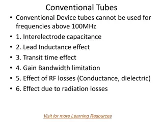
Transferred Electron Devices (TED)
•
Gunn Diode
•
Gunn Effect
Transferred Electron Devices (TED)
•
TED’s are semiconductor devices with no
junctions and gates.
•
They are fabricated from compound
semiconductors like GaAs, InP, CdTe etc.
•
TED’s operate with hot electrons whose
energy is much greater than the thermal
energy.
Gunn Diode
Invented by J.B Gunn
Gunn Effect
•
Above some critical voltage (Corresponding to
Electric field of 2k-4k V/cm)
the current passing
through n-type GaAs becomes a periodic
fluctuating function of time.
•
Frequency of oscillation is determined mainly by
the specimen, not by the external circuit.
•
Period of oscillation is inversely proportional to
the specimen length and is equal to the transit
time of electrons between the electrodes
•
The current waveform was produced by
applying a voltage pulse of 16V and 10ns
duration to an n-type GaAs of 2.5 x 10
-3
cm
length. The oscillation frequency was 4.5Ghz
RWH Theory
•
Explanation for Gunn Effect:
Ridley – Watkins – Hilsum (RWH) Theory
•
Two concepts related with RWH Theory.
–
Differential negative resistance
–
Two valley model
Differential negative resistance
•
Fundamental concept of RWH Theory.
•
Developed in bulk solid state III-V compound
when a voltage is applied
•
Differential negative resistance make the
sample electrically unstable.
Two valley model theory
Electron transfer mechanism
•
Conductivity of n-type GaAs:
•
e
= Electron charge
•
μ
= Electron mobility
•
= Electron density in the lower valley
•
= Electron density in the upper valley
•
is the electron density
Modes of Operation
•
Gunn Oscillation Mode:
–
(f x L) = 10
7
cm/s and (n x L) > 10
12
/cm
2
–
Cyclic formation of High field domain
•
Stable Amplification Mode
–
(f x L) = 10
7
cm/s and 10
11
/cm
2
< (n x L) >10
12
/cm
2
•
LSA Oscillation Mode
–
(f x L) >10
7
cm/s and 2 x 10
4
< (n/f) > 2 X10
5
/cm
2
•
Bias-circuit
–
(f x L) is small. L is very small. When E=E
th
current falls as Gunn
oscillation begins, leads to oscillation in bias circuit (1KHz to
100MHz)
Gunn Oscillation Mode
•
Condition for successful domain drift:
Transit time (L/v
s
) > Electric relaxation time
•
Frequency of oscillation =
v
dom
/L
eff
.
•
Gunn diode with a resistive circuit -> Voltage change
across diode is constant-> Period of oscillation is the
time required for the domain to drift from the cathode
to anode. Not suitable for microwave applications
because of low efficiency.
•
Gunn diode with a resonant circuit has high efficiency.
•
There are three domain modes for Gunn
oscillation modes.
1. Transit time domain mode, (Gunn mode)
2. Delayed domain mode
–
Here domain is collected while
–
Also called inhibited mode.
–
Efficiency: 20%
3. Quenched domain mode:
–
If bias field drops below E
s
, domain collapses
before it reaches anode.
–
When the bias field swings above E
th
, a new
domain starts and process repeats.
–
Frequency of oscillation is determined by resonant
circuit.
–
Efficiency : 13%
•
Limited Space charge Accumulation Mode
(LSA)
Most Important mode for Gunn oscillator.
Domain is not allowed to form.
Efficiency : 20%
Gunn Characteristics
•
Power: 1W (Between 4HHz and 16GHz)
•
Gain Bandwidth product : >10dB
•
Average gain : 1 – 12 dB
•
Noise figure : 15 dB
A
v
a
l
a
n
c
h
e
T
r
a
n
s
i
t
T
i
m
e
D
e
v
i
c
e
s
R
e
l
y
o
n
t
h
e
e
f
f
e
c
t
o
f
v
o
l
t
a
g
e
b
r
e
a
k
d
o
w
n
a
c
r
o
s
s
a
r
e
v
e
r
s
e
b
i
a
s
e
d
p
-
n
j
u
n
c
t
i
o
n
.
•
Two distinct modes of avalanche oscillator is
observed i) IMPATT(impact ionization avalanche
transit time operation)
•
Dc-to-RF c.e is 5 to 10%
•
ii) TRAPPAT (Trapped plasma avalanche triggered
transit operation). 20 to 60%
•
Another type of active microwave device is
BARITT (barrier injected transit time diode)
IMPATT DIODE
•
Electron–hole pairs are generated in the high
field region.
•
The generated
electron
immediately moves into
the
N region
, while the generated
holes
drift
across the
P region
.
•
The time required for the hole to reach the
contact constitutes the
transit time delay
.
•
The Read diode consists of two regions (i) The
Avalanche region (a region with relatively
high
doping
and high field) in which avalanche
multiplication occurs and (ii) the drift region (a
region with essentially intrinsic doping and
constant field) in which the generated holes drift
towards the contact.
•
Read diode is the basic type in the IMPATT diode
family
•
very high doping
•
i or v intrinsic material
•
The space between n+ -p junction and the i –p+
junction is called the space charge region
•
The diode is reverse biased and mounted in a
microwave cavity. The impedance of the cavity is
mainly inductive which is matched with the
capacitive impedance of the diode to form a
resonant circuit.
•
Such device can produce a negative ac resistance
that in turns delivers power from the dc bias to
the oscillation
BAR
rier
I
njection
T
ransit
T
ime Devices
(BARITTs)
•
The injected carrier density increases with the ac voltage. Then the carriers will
traverse the drift region.
The injected hole pulse at 90
o
and the corresponding induced current which travels
3/4s of a cycle to reach the negative terminal. Or w/v
s
= ¾ (1/f)
•
Both the ac voltage and external current are positive therefore ac power is
dissipated in the device.
•
Consequently, the BARITT diodes have low power capabilities and low efficiencies
but they also have low noise (avoiding the avalanche phenomena).
Parametric Devices
•
Uses
non linear reactance
or
time varying reactance
•
Parametric
term is derived from parametric excitation,
since the capacitance or inductance, which is a
reactive
parameter
, can be used to
produce capacitive or
inductive excitation.
•
Parametric excitation is subdivided into
parametric
amplification and oscillation
.
•
Many
of the essential
properties
of non linear energy
storage systems were described by Faraday and Lord
Rayleigh.
•
Derived a set of general energy relations
regarding power flowing into and out of an ideal
nonlinear reactance.
•
These relations are useful in predicting whether
power gain is possible in a parametric amplifier.
•
One signal generator and one pump generator at their
respective frequencies , together with associated series
resistances and bandpass filters, are applied to a nonlinear
capacitance C(t).
•
These resonating circuits of filters are designed to reject
power at all frequencies other than their respective signal
frequencies.
•
In the presence of two applied frequencies an infinite number
of resonant frequencies of are generated, where m and n are
any integers.
•
Each of the resonating circuits is assumed to be ideal.
•
The power loss by the nonlinear susceptance is
negligible. That is the power entering the nonlinear
capacitor at the pump frequency is equal to the
power leaving the capacitor at the other frequencies
through the nonlinear interaction.
•
Manley and Rowe established the power relations
between the input power at the frequencies and the
output power at the other frequencies
Device Power Output vs Frequency
Explore the world of microwave diodes and transfer electron devices (TED) in radar technology. Learn about Gunn diodes, Gunn effect, RWH theory, and differential negative resistance. Discover how TEDs operate with hot electrons and the critical voltages involved. Dive into the fascinating concepts behind the oscillation frequencies and sample instability in these semiconductor devices.

Download Presentation

Please find below an Image/Link to download the presentation.
The content on the website is provided AS IS for your information and personal use only. It may not be sold, licensed, or shared on other websites without obtaining consent from the author. Download presentation by click this link. If you encounter any issues during the download, it is possible that the publisher has removed the file from their server.
E N D
Presentation Transcript
Subject Name: Microwave and Radar Subject Code: 10EC54 Prepared By: Lakshmi C R, Dharani K G Department: ECE Date: 10.11.14 22/8/14
UNIT 3 MICROWAVE DIODES AND TRANSFER ELECTRON DEVICES
TOPICS COVERED Transferred Electron Devices (TED) Gunn Diode Gunn Effect
Transferred Electron Devices (TED) TED s are semiconductor devices with no junctions and gates. They semiconductors like GaAs, InP, CdTe etc. are fabricated from compound TED s operate with hot electrons whose energy is much greater than the thermal energy.
Gunn Diode Invented by J.B Gunn
Gunn Effect Above some critical voltage (Corresponding to Electric field of 2k-4k V/cm) the current passing through n-type GaAs becomes a periodic fluctuating function of time. Frequency of oscillation is determined mainly by the specimen, not by the external circuit. Period of oscillation is inversely proportional to the specimen length and is equal to the transit time of electrons between the electrodes
The current waveform was produced by applying a voltage pulse of 16V and 10ns duration to an n-type GaAs of 2.5 x 10⁻³ cm length. The oscillation frequency was 4.5Ghz
RWH Theory Explanation for Gunn Effect: Ridley Watkins Hilsum (RWH) Theory Two concepts related with RWH Theory. Differential negative resistance Two valley model
Differential negative resistance Fundamental concept of RWH Theory. Developed in bulk solid state III-V compound when a voltage is applied
Differential negative resistance make the sample electrically unstable.
Conductivity of n-type GaAs: e = Electron charge = Electron mobility = Electron density in the lower valley = Electron density in the upper valley is the electron density
Modes of Operation Gunn Oscillation Mode: (f x L) = 107 cm/s and (n x L) > 1012 /cm2 Cyclic formation of High field domain Stable Amplification Mode (f x L) = 107 cm/s and 1011/cm2 < (n x L) >1012/cm2 LSA Oscillation Mode (f x L) >107 cm/s and 2 x 10⁴ < (n/f) > 2 X10⁵/cm2 Bias-circuit (f x L) is small. L is very small. When E=Eth current falls as Gunn oscillation begins, leads to oscillation in bias circuit (1KHz to 100MHz)
Gunn Oscillation Mode Condition for successful domain drift: Transit time (L/vs) > Electric relaxation time Frequency of oscillation = vdom/Leff. Gunn diode with a resistive circuit -> Voltage change across diode is constant-> Period of oscillation is the time required for the domain to drift from the cathode to anode. Not suitable for microwave applications because of low efficiency. Gunn diode with a resonant circuit has high efficiency.
There are three domain modes for Gunn oscillation modes. 1. Transit time domain mode, (Gunn mode)
2. Delayed domain mode Here domain is collected while Also called inhibited mode. Efficiency: 20%
3. Quenched domain mode: If bias field drops below Es, domain collapses before it reaches anode. When the bias field swings above Eth, a new domain starts and process repeats. Frequency of oscillation is determined by resonant circuit. Efficiency : 13%
Limited Space charge Accumulation Mode (LSA) Most Important mode for Gunn oscillator. Domain is not allowed to form. Efficiency : 20%
Gunn Characteristics Power: 1W (Between 4HHz and 16GHz) Gain Bandwidth product : >10dB Average gain : 1 12 dB Noise figure : 15 dB
Avalanche Transit Time Devices Rely on the effect of voltage breakdown across a reverse biased p-n junction. Two distinct modes of avalanche oscillator is observed i) IMPATT(impact ionization avalanche transit time operation) Dc-to-RF c.e is 5 to 10% ii) TRAPPAT (Trapped plasma avalanche triggered transit operation). 20 to 60% Another type of active microwave device is BARITT (barrier injected transit time diode)
Electronhole pairs are generated in the high field region. The generated electron immediately moves into the N region, while the generated holes drift across the P region. The time required for the hole to reach the contact constitutes the transit time delay.
The Read diode consists of two regions (i) The Avalanche region (a region with relatively high doping and high field) in which avalanche multiplication occurs and (ii) the drift region (a region with essentially intrinsic doping and constant field) in which the generated holes drift towards the contact. Read diode is the basic type in the IMPATT diode family very high doping i or v intrinsic material
The space between n+ -p junction and the i p+ junction is called the space charge region The diode is reverse biased and mounted in a microwave cavity. The impedance of the cavity is mainly inductive which is matched with the capacitive impedance of the diode to form a resonant circuit. Such device can produce a negative ac resistance that in turns delivers power from the dc bias to the oscillation
BARrier Injection Transit Time Devices (BARITTs) The injected carrier density increases with the ac voltage. Then the carriers will traverse the drift region. The injected hole pulse at 90o and the corresponding induced current which travels 3/4s of a cycle to reach the negative terminal. Or w/vs = (1/f) Both the ac voltage and external current are positive therefore ac power is dissipated in the device. Consequently, the BARITT diodes have low power capabilities and low efficiencies but they also have low noise (avoiding the avalanche phenomena).
Parametric Devices Uses non linear reactance or time varying reactance Parametric term is derived from parametric excitation, since the capacitance or inductance, which is a reactive parameter, can be used to produce capacitive or inductive excitation. Parametric excitation is subdivided into parametric amplification and oscillation. Many of the essential properties of non linear energy storage systems were described by Faraday and Lord Rayleigh.
Derived a set of general energy relations regarding power flowing into and out of an ideal nonlinear reactance. These relations are useful in predicting whether power gain is possible in a parametric amplifier.
One signal generator and one pump generator at their respective frequencies , together with associated series resistances and bandpass filters, are applied to a nonlinear capacitance C(t). These resonating circuits of filters are designed to reject power at all frequencies other than their respective signal frequencies. In the presence of two applied frequencies an infinite number of resonant frequencies of are generated, where m and n are any integers.
Each of the resonating circuits is assumed to be ideal. The power loss by the nonlinear susceptance is negligible. That is the power entering the nonlinear capacitor at the pump frequency is equal to the power leaving the capacitor at the other frequencies through the nonlinear interaction. Manley and Rowe established the power relations between the input power at the frequencies and the output power at the other frequencies


")


 The")
 The")