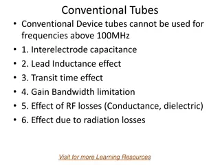
Comprehensive Microwave Circuit Design Course Overview
This comprehensive course on Microwave Circuit Design by Professor Syed Idris Syed Hassan covers topics such as transmission lines, network parameters, matching techniques, power dividers, diode circuits, amplifiers, oscillators, filters design, and more. The syllabus includes lectures, simulations, assessments, and exams. References include renowned texts on microwave engineering. The course provides a detailed analysis of transmission lines, equivalent circuits, and Kirchoff's laws. Scheduled class dates and timings are provided for convenience.

Download Presentation

Please find below an Image/Link to download the presentation.
The content on the website is provided AS IS for your information and personal use only. It may not be sold, licensed, or shared on other websites without obtaining consent from the author.If you encounter any issues during the download, it is possible that the publisher has removed the file from their server.
You are allowed to download the files provided on this website for personal or commercial use, subject to the condition that they are used lawfully. All files are the property of their respective owners.
The content on the website is provided AS IS for your information and personal use only. It may not be sold, licensed, or shared on other websites without obtaining consent from the author.
E N D
Presentation Transcript
Microwave Circuit Design By Professor Syed Idris Syed Hassan Sch of Elect. & Electron Eng Engineering Campus USM Nibong Tebal 14300 SPS Penang
Introduction 10 weeks lecture + 4 weeks ADS simulation Assessments :8 tests + 2 ADS assignments + 1 final examination Class : 9.00- 10.30 lecture 10.30-11.00 rest (tea break) 11.00-12.30 lecture 12.30- 1.00 test
Dates 06/04/02 Morning 20/04/02 Morning 27/04/02 Morning 04/05/02 Morning 11/05/02 Morning 18/05/02 Morning 25/05/02 Morning 08/06/02 Morning 15/06/02 Morning 22/06/02 Morning 29/06/02 morning 06/07/02 Morning 20/07/02 Morning 27/07/02 Morning
Syllabus Transmission lines Network parameters Matching techniques Power dividers and combiners Diode circuits Microwave amplifiers Oscillators Filters design Applications Miscellaneous
References David M Pozar ,Microwave Engineering- 2nd Ed., John Wiley , 1998 E.H.Fooks & R.A.Zakarevicius, Microwave Engineering using microstrip circuits, Prentice Hall,1989. G. D. Vendelin, A.M.Pavio &U.L.Rohde, Microwave circuit design-using linear and Nonlinear Techniques, John Wiley, 1990. W.H.Hayward, Introduction to Radio Frequency Design, Prentice Hall, 1982.
Equivalent Circuit z R L R L C G + R j L ( )( ) = + + R j L G j C = Zo Lossy line + G j C L = LC Zo= Lossless line C
Analysis dI ( t z , ) I + + I z R j L dz dV + ( t z , ) V V z + G j C dz Kirchoff current law dI = From Kirchoff Voltage Law dV dV dI + + I I z GV z C z + = + V V z RI z L z dz dt dz dt dI dV dV dI = + z GV z C z = + z RI z L z dz dt dz dt dV dI dI dV (b) (a) = + = + RI L GV C dz dt dz dt
Analysis dI dV = j I = then j V Let s V=Voej t , I = Ioej t dt dt Therefore dI ( )V dV = + ( )I b G j C = + R j L a dz dz Differentiate with respect to z ( R dz 2 d I 2 dV ( )dz = + G j C 2 d V 2 dI )dz dz = + j L 2 2 d V 2 d I 2 ( )( )V ( )( )I = + + = + + R j L G j C R j L G j C dz dz 2 d V 2 2 d I 2 = 2 V = 2 I dz dz
Analysis The solution of V and I can be written in the form of o Z + = Be Ae V c d = I + z z Be Ae + z z where + ( )( ) R j L = + = + + and j R j L G j C = Zo + G j C Let say at z=0 , V=VL , I=IL and Z=ZL Therefore B o Z f VL L + = V A e = I B A L = Z L and I L
Analysis Solve simultaneous equations ( e ) and (f ) 2 I 2 I = B = A o L L Z V o L L + Z V Inserting in equations ( c) and (d) we have + + z z z z + 2 2 e e e e = ( ) V z V I Z L L o + + z z z z + 2 2 e e V e e L = ( ) I z I L Z o
Analysis + 2 z z 2 e e z z e e = and sinh( ) z = cosh( ) z But Then, we have * = ( ) cosh( ) sinh( ) V z V z I Z z L L o V ** L = ( ) cosh( ) sinh( ) I z I z z L Z o cosh( ) sinh( ) ( ) V z I Z z V z L L o = = ( ) Z z and V ( ) I z L cosh( ) sinh( ) I z z L Z o
Analysis cosh( ) sinh( ) Z z Z z L o = ( ) Z z Z or o cosh( ) sinh( ) Z z Z z o L tanh( ) Z Z z Or further reduce L o = ( ) Z z Z o tanh( ) Z Z z o L For lossless transmission line , = j since = = cosh( ) cos( ) j z z + tan( ) Z jZ z L o = ( ) Z z Z o = + sinh( ) sin( ) j z j z tan( ) Z jZ z o L
Analysis antinode Standing Wave Ratio (SWR) Reflection coefficient node z Be = z Ae Ae- z Be z Voltage and current in term of reflection coefficient ( ) + z z z 1 V = + = + 1 V Ae Be Ae L = = Z Z L L o + 1 I L z z z Ae Be Ae 1 Z ( ) = = or L 1 I = L Z Z 1 Z o o o
Analysis = j For loss-less transmission line By substituting in * and ** ,voltage and current amplitude are cos( 2 1 ) ( + + = A z V 2 1 ) ( + = Z o Voltage at maximum and minimum points are + = A V and g / 1 ) 2 2 + 2 z / 1 ) 2 A 2 + cos( 2 I z z h = A 1 ( ) 1 ( ) V max min + 1 Z Therefore = = VSWR s L s = For purely resistive load 1 Z o
Analysis Other related equations 1 Z V + 1 V min o = = = Z Z max = = = Z Z sZ min o + max o o 1 I s 1 I max min Z Z L o = + Z Z L o From equations (g) and (h), we can find the max and min points + = 2 , 0 2 , 4 , z Maximum + = 2 , 3 , z Minimum
Important Transmission line equations Zin ZL Zo + tanh Z jZ L o = Z Z in o + tanh Z jZ o L Z Z + 1 L o = =1 SWR + Z Z L o
Various forms of Transmission Lines Two wire cable Microstripe line Coaxial cable Rectangular waveguide Circular waveguide Stripline
Parallel wire cable = C or for a d ( ) ( ) cosh1 ln / d a / 2 d a ( ) ( ) cosh1 = / 2 ln / L d a or d a for a d 1 ( ) 1 = cosh / 2 Zo d a Where a = radius of conductor d = separation between conductors
Coaxial cable b ( ) = ln / L b a a 2 2 ck 2 2 = C c = f ( ) ln / c b a r 1 ( ) = ln / Zo b a = kc 2 + a b Where a = radius of inner conductor b = radius of outer conductor c = 3 x 10⁸ m/s
Micro strip Conducted strip t Substrate r he w Ground t=thickness of conductor
Characteristic impedance of Microstrip line 60 1 / = / 12 1 2 2 ( ) h / + ln 8 / . 0 25 For w h Z h w w o e e eff + 1 1 ( ) ( ) 5 . 0 2 r r = + + + . 0 04 1 / h w w h eff e e 377 + = / 1 For w h Z ( ) o . 1 + . 1 + / 393 . 0 667 ln / 444 w h w h eff 1 e e + 1 ( ) 5 . 0 r r = + + 1 12 / h w eff e 2 2 w=width of strip h=height and t=thickness 2 t h e = = + + Where 2 he h t ln 1 w w e t
Microstrip width 2 / 1 + 2 1 1 . 0 11 Z 60 o r r = + + . 0 23 A + 1 r r 2 60 = B Z o r 8 exp( ) A = For A>1.52 / W h exp( 2 ) 2 A For A<1.52 2 1 . 0 61 ( ) ( ) r 2 = + + / 1 ln 2 1 1 . 0 39 W h B B lb B r r
Simple Calculation 377 w = Z o + 2 r h Approximation only 377 rZ = / 2 w h o
Microstrip components Capacitance Inductance Short/Open stub Open stub Transformer Resonator
Capacitance Zoc Zo Zo = C For 8 Z 1c oc 2 8 3 10 = sin C For = / c m s 1 2 Z c 8 1 oc r
Inductance ZoL Zo Zo Z oL = L For 8 1c 8 3 10 Z For oL = = / c m s sin L 1 8 c 1 r
Short Stub Zo Zo Zo ZL Z = = + tan Z X jZ sc L o ( ) tan1 = o LZ X / = o 360 eff
Open stub Zo Zo Zo ZL Z = = cot Z X jZ oc c o ( ) cot1 = cZ X / o = o 360 eff
Quarter-wave transformer x ZT ZL Zo Zo Zmx/min At maximum point 1 Z Z L o =1 = = s + + Z Z L 2 o = ( ) Z x Z s = in radian x max o = = = Z . Z Z Z Z s Z s T in mx o o o
Quarter-wave transformer at minimum point Z Z 1 L o = = =1 s + Z Z + L o + min= ( ) o/ Z x Z s = x in radian 2 = = = Z . / / Z Z Z Z s Z s min T in o o o
Resonator Circular microstrip disk Circular ring Short-circuited /2 lossy line Open-circuited /2 lossy line Short-circuited /4 lossy line
Circular disk/ring feeding a . 1 841 o = a 2 r a = a 4 * These components usually use for resonators
Short-circuited /2 lossy line Zin = series RLC resonant cct Zo =n /2 R = o Z L o = = = Q 2 2 R Z 2 o = L 1 o 2 = C = where 2 L o
Open-circuited /2 lossy line Zin = parallel RLC resonant cct Zo =n /2 Z o R = = = = Q RC o 2 2 = C 2 oZ 1 2 o = where = L 2 C o
Short-circuited /4 lossy line Zin = parallel RLC resonant cct Zo = /4 Z o R = = = = Q RC o 4 2 = C 4 oZ 1 2 o = where = L 2 C o
Rectangular waveguide b g = a Z TE Cut-off frequency of TE or TM mode o o 2 2 = Z 1 m n TM = + fcmn g a b 2 Conductor attenuation for TE10 ( ) 1 1 1 R 2 3 2 s = + 2 / b a Np m = c o 3 2 2 2 a b g o g o c o R = s 2
Example Given that a= 2.286cm , b=1.016cm and = x S/m. What are the mode and attenuation for 10GHz? Using this equation to calculate cutoff frequency of each mode 2 2 1 m n = + fcmn a b 2
Calculation TE10 a=2.286mm, b=1.016mm, m=1 and n=0 ,thus we have 2 8 3 10 9 = = . 6 562 10 fc GHz 10 2 002286 . 0 Similarly we can calculate for other modes
Example TE20 TE01 TE11 TE10 Mode fcmn TE10 6.562 GHz 6.562GHz 13.123GHz14.764GHz 16.156GHz TE20 13.123GHz Frequency 10Ghz is propagating in TE10.mode since this frequency is below the 13.123GHz (TE20) and above 6.561GHz (TE10) TE01 14.764GHz TE11 16.156GHz
continue 2 1 = = 158 05 . m o a o = = . 0 026 R s 2 ( ) R 2 3 2 s = + = 2 . 0 0125 / b a Np m c o 3 a b g o or = = ( ) 20 log . 0 11 / dB e dB m c c
Evanescent mode Mode that propagates below cutoff frequency of a wave guide is called evanescent mode Wave propagation constant is 2 2 2 o = + c k Where kc is referred to cutoff frequency, is referred to propagation in waveguide and is in space When f0< fc , 2 2 2 o = c k = +j =attenuation =phase constant But 1 1 = 2 Since no propagation then 2 2 c o The wave guide become attenuator
Cylindrical waveguide n p'n1 p'n2 p'n3 0 3.832 7.016 10.174 1 1.841 5.331 8.536 a 2 3.054 6.706 9.97 TE mode Dominant mode is TE11 , , p g p = Z nm = k nm = f TE cnm cnm a R a 2 o 2 o 2 s = + k 11 c c '2 11 2 o 2 cnm a = 1 p k o g nm
continue n pn1 pn2 pn3 0 2.405 5.520 8.654 a 1 3.832 7.016 10.174 2 5.135 8.417 11.620 TM mode p nm p cnm= o k = Z nm = f TM a cnm a 2 g TM01 is preferable for long haul transmission 2 o 2 cnm k = nm
Example Find the cutoff wavelength of the first four modes of a circular waveguide of radius 1cm 2nd mode Refer to tables TM modes TE modes n p'n1 p'n2 p'n3 n pn1 pn2 pn3 0 2.405 5.520 8.654 0 3.832 7.016 10.174 1 3.832 7.016 10.174 1 1.841 5.331 8.536 2 5.135 8.417 11.620 2 3.054 6.706 9.97 3rd &4th modes modes 3rd &4th 1st mode
Calculation p 2 a nm = f = cnm cnm a 2 p nm . 0 2 01 = = 0341 . 0 m 1st mode Pnm= 1.841, TE11 11 c . 1 841 . 0 2 01 = = 0261 . 0 m 2nd mode Pnm= 2.405, TM01 01 c . 2 405 1st mode Pnm= 3.832, TE01 and TM11 . 0 2 01 = = = 0164 . 0 m 01 11 c c . 3 832
Stripline b w 30 b = Z ( ) b o + . 0 441 W r e W = . 0 35 We W b We W W ( . 0 ) 2 = 35 / . 0 35 W b b b b
Continue On the other hand we can calculate the width of stripline for a given characteristic impedance 30 W = . 0 441 120 for Z r o b Z r o 30 W = . 0 85 6 . 0 . 0 441 120 for Z r o b Z r o
Continue 3 30 R 7 . 2 10 R Z s r o 120 A for Z ( ) r o b t = c . 0 16 Z s 120 B for Z r o b o Where + t 414 2 2 W b t b t = + + 1 ln + A ( ) b t b t 4 . 0 1 b t W = + + 1 5 . 0 ln B ( 5 . 0 ) + 2 7 . 0 W t W t t =thickness of the strip