CMOS Chip Testing: Need, Principles, Strategies
This content delves into the critical aspects of CMOS chip testing, highlighting the necessity, testing principles, design strategies, and techniques at the chip and system levels. It also explores layout design for enhanced testability, logic verification, silicon debugging, manufacturing testing, and common chip failures.

Download Presentation

Please find below an Image/Link to download the presentation.
The content on the website is provided AS IS for your information and personal use only. It may not be sold, licensed, or shared on other websites without obtaining consent from the author.If you encounter any issues during the download, it is possible that the publisher has removed the file from their server.
You are allowed to download the files provided on this website for personal or commercial use, subject to the condition that they are used lawfully. All files are the property of their respective owners.
The content on the website is provided AS IS for your information and personal use only. It may not be sold, licensed, or shared on other websites without obtaining consent from the author.
E N D
Presentation Transcript
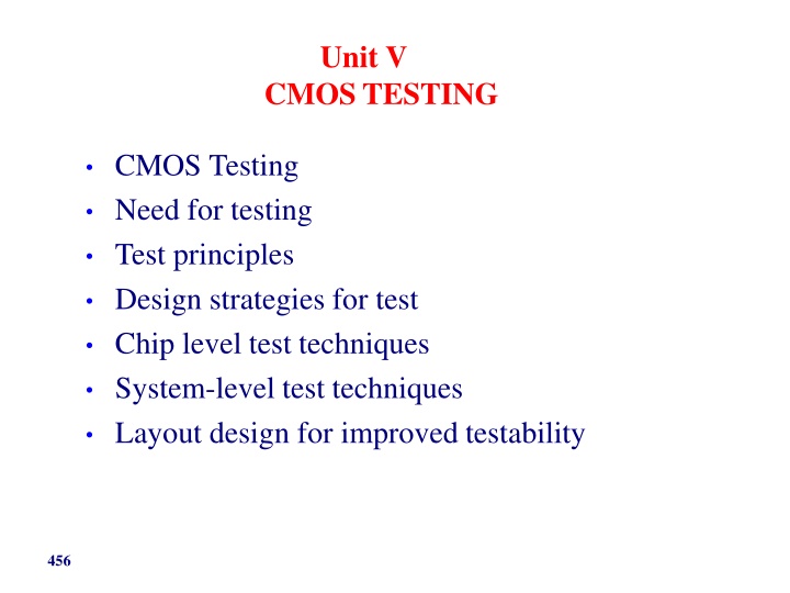
Unit V CMOS TESTING CMOS Testing Need for testing Test principles Design strategies for test Chip level test techniques System-level test techniques Layout design for improved testability 456
Need for Testing Testing is one of the most expensive parts of chips Logic verification accounts for > 50% of design effort formany chips Debug time after fabrication has enormous opportunitycost Shipping defective parts can sink acompany Example: Intel FDIV bug (1994) Logic error not caught until > 1M unitsshipped Recall cost $450M (!!!) 457
Logic Verification Does the chip simulate correctly? Usually done at HDLlevel Verification engineers write test bench forHDL Can t test allcases Look for cornercases Try to break logicdesign Ex: 32-bit adder Test all combinations of corner cases asinputs: 0, 1, 2, 231-1, -1, -231, a few random numbers Good tests require ingenuity 458
Silicon Debug Test the first chips back from fabrication If you are lucky, they work the firsttime If not Logic bugs vs. electrical failures Most chip failures are logic bugs from inadequatesimulation Some are electrical failures Crosstalk Dynamic nodes: leakage, chargesharing Ratiofailures A few are tool or methodology failures (e.g.DRC) Fix the bugs and fabricate a corrected chip 459
Manufacturing Test A speck of dust on a wafer is sufficient to kill chip Yield of any chip is < 100% Must test chips after manufacturing before delivery to customersto only ship good parts Manufacturing testers are very expensive Minimize time on tester Careful selectionof test vectors 460
Manufacturing Failures SEM images courtesy Intel Corporation 461
Stuck-At Faults How does a chip fail? Usually failures are shorts between two conductors or opens ina conductor This can cause very complicatedbehavior A simpler model: Stuck-At Assume all failures cause nodes to be stuck-at 0 or 1, i.e.shorted to GND or VDD Not quite true, but works well inpractice 462
Examples 463
Observability & Controllability Observability: ease of observing a node by watching external output pins of the chip Controllability: ease of forcing a node to 0 or 1 by driving input pins of the chip Combinational logic is usually easy to observe and control Finite state machines can be very difficult, requiring many cycles to enter desired state Especially if state transition diagram is not known to thetest engineer 464
Test Pattern Generation Manufacturing test ideally would check every node in the circuit to prove it is not stuck. Apply the smallest sequence of test vectors necessary to prove each node is not stuck. Good observability and controllability reduces number of test vectors required for manufacturing test. Reduces the cost of testing Motivates design-for-test 465
Test Example SA1 SA0 {11 A310} A2 1110} 01 A010} {0110} A3 A2 A1 A0 n1 n2 n3 Y n1 {1010} {0100} {0110} {1110} {0110} {0101} {0110} { { { { { { {1110} Y n2 n3 A1 0111} 0110} 0100} 0110} Minimum46s6et: {0100, 0101, 0110, 0111, 1010,
Design for Test Design the chip to increase observability and controllability If each register could be observed and controlled, test problem reduces to testing combinational logic between registers. Better yet, logic blocks could enter test mode where they generate test patterns and report the results automatically. 467
Scan Convert each flip-flop to a scan register Only costs one extramultiplexer Normal mode: flip-flops behave as usuaSlI CLK SCAN Flop Q D Scan mode: flip-flops behave as shift register scan-in Contents of flops can be scanned out and new values scanned in Flop Flop Flop Flop Flop Flop Logic Cloud Logic Cloud inputs outputs Flop Flop Flop Flop Flop Flop scanout 468
Scannable Flip-flops SCAN SCAN CLK Q D D 0 X Q Flop Q SI 1 SI (a) (b) d D Q d SCAN d X Q s s SI (c) s 469
ATPG Test pattern generation is tedious Automatic Test Pattern Generation (ATPG) tools produce a good set of vectors for each block of combinational logic Scan chains are used to control and observe the blocks Complete coverage requires a large number of vectors, raising the cost of test Most products settle for covering 90+% of potential stuck-at faults 470
Built-in Self-test Built-in self-test lets blocks test themselves Generate pseudo-random inputs to comb.logic Combine outputs into a syndrome With high probability, block is fault-free if it producesthe expected syndrome 471
PRSG Linear Feedback Shift Register Shift register with input taken from XOR ofstate Pseudo-Random SequenceGenerator Step 0 1 2 3 4 5 6 7 Y Y CLK 111 110 101 010 100 001 011 111(repeats) Q[2] Q[0] Q[1] Flop Flop Flop D D D Flops reset to 111 472
BILBO Built-in Logic Block Observer Combine scan with PRSG & signatureanalysis D[0] D[1] D[2] C[0] C[1] Q[2] / SO Flop Flop Flop SI 1 Q[0] 0 Q[1] MODE Scan Test Reset Normal C[1] 0 0 1 1 C[0] 0 1 0 1 Logic Cloud Signature Analyzer PRSG 473
Boundary Scan Testing boards is also difficult Need to verify solder joints aregood Drive a pin to 0, then to1 Check that all connected pins get thevalues Through-hold boards used bed of nails SMT and BGA boards cannot easily contact pins Build capability of observing and controlling pins into each chip to make board test easier 474
Boundary Scan Example PackageInterconnect CHIPB CHIPC SerialDataOut CHIPA CHIPD IOpadandBoundaryScan Cell SerialDataIn 475
Boundary Scan Interface Boundary scan is accessed through five pins TCK: TMS: TDI: TDO: TRST*: test reset (optional) test clock test modeselect test data in test dataout Chips with internal scan chains can access the chains through boundary scan for unified test strategy. 476
Summary Think about testing from the beginning Simulate as you go Plan for test after fabrication If you don t test it, it won t work! (Guaranteed) 477