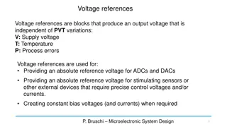
Overview of CMOS Process in Microelectronic Design
The CMOS Process
P. Bruschi – Microelectronic System Design
1
•
P
l
a
n
a
r
C
M
O
S
p
r
o
c
e
s
s
i
s
u
s
e
d
u
p
t
o
t
h
e
2
8
n
m
t
e
c
h
n
o
l
o
g
y
n
o
d
e
.
•
F
o
r
l
a
t
e
r
t
e
c
h
n
o
l
o
g
y
n
o
d
e
s
,
3
D
C
M
O
S
M
O
S
F
E
T
s
(
F
i
n
F
E
T
s
)
a
r
e
u
s
e
d
.
•
P
l
a
n
a
r
C
M
O
S
p
r
o
c
e
s
s
e
s
a
r
e
s
t
i
l
l
e
x
t
e
n
s
i
v
e
l
y
u
s
e
d
f
o
r
a
n
a
l
o
g
a
n
d
m
i
x
e
d
-
s
i
g
n
a
l
I
C
s
.
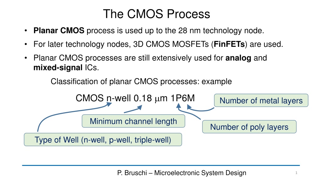
Classification of planar CMOS processes: example
CMOS n-well 0.18
m 1P6M
Minimum channel length
Type of Well (n-well, p-well, triple-well)
Number of poly layers
Number of metal layers
Simplified designer's view of a CMOS Process
P. Bruschi – Microelectronic System Design
2
•
We are considering a simple n-well (twin-Tub) 1P2M process
•
T
h
e
s
t
a
r
t
i
n
g
s
u
b
s
t
r
a
t
e
i
s
p
-
t
y
p
e
:
a
l
l
p
-
w
e
l
l
s
a
r
e
s
h
o
r
t
e
d
t
o
g
e
t
h
e
r
s
i
n
c
e
t
h
e
r
e
a
r
e
n
o
i
n
s
u
l
a
t
i
o
n
j
u
n
c
t
i
o
n
s
w
i
t
h
t
h
e
s
u
b
s
t
r
a
t
e
.
•
N-wells are insulated from the substrate if the latter is biased at the
lowest voltage in the circuit.
•
A very lightly doped epitaxial layer is often present on top of a strongly
doped wafer. P-wells are necessary to obtain the optimal doping for n-
MOSFETS.
The active areas
P. Bruschi – Microelectronic System Design
3
Top view
•
Active areas are all
of the same type.
•
They are
specialized
by other
layers (e.g. n-well).
•
p
-
w
e
l
l
s
a
r
e
o
f
t
e
n
d
r
a
w
n
a
u
t
o
m
a
t
i
c
a
l
l
y
a
s
n
o
t
(
n
-
w
e
l
l
)
n-well
Polysilicon and gate oxide
P. Bruschi – Microelectronic System Design
4
•
T
h
e
g
a
t
e
(
t
h
i
n
)
o
x
i
d
e
i
s
g
r
o
w
n
o
n
a
l
l
a
c
t
i
v
e
a
r
e
a
s
.
•
After that, it is covered by the polysilicon layer
•
When the poly is patterned, the gate oxide remains only where
polysilicon remains, forming the gate.
•
Only one layer (poly) is required to control the final result of this step.
poly over active area
MOSFET gate
poly out of active area
inteconnection
FEOL (Front-End Of the Line)
P. Bruschi – Microelectronic System Design
5
BEOL (Back End Of the Line) - Contacts
P. Bruschi – Microelectronic System Design
6
•
A
l
l
d
e
v
i
c
e
s
c
r
e
a
t
e
d
i
n
t
h
e
F
E
O
L
a
r
e
c
o
v
e
r
e
d
b
y
a
n
i
n
s
u
l
a
t
i
n
g
l
a
y
e
r
a
n
d
h
o
l
e
s
a
r
e
o
p
e
n
e
d
o
n
l
y
w
h
e
r
e
w
e
w
a
n
t
t
o
c
o
n
t
a
c
t
t
h
e
m
.
T
h
e
s
e
o
p
e
n
i
n
g
a
r
e
t
h
e
C
O
N
T
A
C
T
S
•
Contacts can reach active areas (p+ or n+ doped portions of the
substrate) or polysilicon (over the FOX).
•
Direct contact of polysilicon over the gates is not allowed
Insulating
Layer
Contacts
Thungsten
Plugs
BEOL: The interconnections
P. Bruschi – Microelectronic System Design
7
Bonding Pads
P. Bruschi – Microelectronic System Design
8
Layer: Passivation Opening
The Triple Well
P. Bruschi – Microelectronic System Design
9
n-well
n-well
n-well twin tub
buried well o buried layer
Triple Well: Multiple PWells and NWells at independent voltages
P. Bruschi – Microelectronic System Design
10
Bipolar processes
P. Bruschi – Microelectronic System Design
11
BiCMOS, BCD, SOI
P. Bruschi – Microelectronic System Design
12
Resistances in planar ICs
P. Bruschi – Microelectronic System Design
13
Direction of the current
/ square
Number of
squares
W
Vertical and lateral capacitances
P. Bruschi – Microelectronic System Design
14
Capacitance per unit area
Capacitance per unit perimeter
(Fringe capacitance)
Area
Perimeter
Lateral and Junction Capacitances
P. Bruschi – Microelectronic System Design
15
Lateral
Junction
p (or n)
n (or p)
The CMOS process involves both planar and 3D CMOS technologies for different technology nodes. Planar CMOS processes, like CMOS n-well 0.18μm 1P6M, are still widely used for analog and mixed-signal ICs. This process includes steps like creating active areas, depositing polysilicon and gate oxide for MOSFETs, Front-End-Of-the-Line (FEOL) processes, Back-End-Of-the-Line (BEOL) with contacts and interconnections. Images illustrate the key stages of the CMOS process in microelectronic system design.

Uploaded on Oct 02, 2024 | 0 Views
Download Presentation

Please find below an Image/Link to download the presentation.
The content on the website is provided AS IS for your information and personal use only. It may not be sold, licensed, or shared on other websites without obtaining consent from the author.If you encounter any issues during the download, it is possible that the publisher has removed the file from their server.
You are allowed to download the files provided on this website for personal or commercial use, subject to the condition that they are used lawfully. All files are the property of their respective owners.
The content on the website is provided AS IS for your information and personal use only. It may not be sold, licensed, or shared on other websites without obtaining consent from the author.
E N D
Presentation Transcript
The CMOS Process Planar CMOS process is used up to the 28 nm technology node. For later technology nodes, 3D CMOS MOSFETs (FinFETs) are used. Planar CMOS processes are still extensively used for analog and mixed-signal ICs. Classification of planar CMOS processes: example CMOS n-well 0.18 m 1P6M Number of metal layers Minimum channel length Number of poly layers Type of Well (n-well, p-well, triple-well) P. Bruschi Microelectronic System Design 1
Simplified designer's view of a CMOS Process We are considering a simple n-well (twin-Tub) 1P2M process The starting substrate is p-type: all p-wells are shorted together since there are no insulation junctions with the substrate. N-wells are insulated from the substrate if the latter is biased at the lowest voltage in the circuit. A very lightly doped epitaxial layer is often present on top of a strongly doped wafer. P-wells are necessary to obtain the optimal doping for n- MOSFETS. P. Bruschi Microelectronic System Design 2
The active areas Active areas are all of the same type. They are specialized by other layers (e.g. n-well). p-wells are often drawn automatically as not(n-well) n-well Top view P. Bruschi Microelectronic System Design 3
Polysilicon and gate oxide poly over active area MOSFET gate poly out of active area inteconnection The gate (thin) oxide is grown on all active areas. After that, it is covered by the polysilicon layer When the poly is patterned, the gate oxide remains only where polysilicon remains, forming the gate. Only one layer (poly) is required to control the final result of this step. P. Bruschi Microelectronic System Design 4
FEOL (Front-End Of the Line) P. Bruschi Microelectronic System Design 5
BEOL (Back End Of the Line) - Contacts All devices created in the FEOL are covered by an insulating layer and holes are opened only where we want to contact them. These opening are the CONTACTS Contacts can reach active areas (p+ or n+ doped portions of the substrate) or polysilicon (over the FOX). Direct contact of polysilicon over the gates is not allowed Contacts Insulating Layer Thungsten Plugs P. Bruschi Microelectronic System Design 6
BEOL: The interconnections P. Bruschi Microelectronic System Design 7
Bonding Pads Layer: Passivation Opening P. Bruschi Microelectronic System Design 8
The Triple Well n-well twin tub n-well n-well buried well o buried layer P. Bruschi Microelectronic System Design 9
Triple Well: Multiple PWells and NWells at independent voltages P. Bruschi Microelectronic System Design 10
Bipolar processes Technology Available Devices Notes Bipolar Vertical NPN, Lateral PNP Used for precision and/or fast amplifier. Si-Ge versions for RF applications Complementary Bipolar Vertical NPN, Vertical PNP BiFet BJTs and JFETs Used for precision / low bias current amplifiers P. Bruschi Microelectronic System Design 11
BiCMOS, BCD, SOI Technology Available Devices Notes BiCMOS CMOS + BJTs Mixed Signal ICs High speed digital line drivers Smart Power BCD Bipolar, CMOS, DMOS SOI Insulator. Silicon on As CMOS, BiCMOS or BCD High Voltage and Rad Hard (e.g. space applications) P. Bruschi Microelectronic System Design 12
Resistances in planar ICs / square Number of squares Direction of the current W L = R R S W P. Bruschi Microelectronic System Design 13
Vertical and lateral capacitances = = Area A P W W W A B + 2 2 W Perimeter A B = k A k P + C V A P Capacitance per unit area Capacitance per unit perimeter (Fringe capacitance) P. Bruschi Microelectronic System Design 14
Lateral and Junction Capacitances n (or p) p (or n) L t Junction = Lateral m C L d d = + C C A C P n p J JSW P. Bruschi Microelectronic System Design 15


")
 - Contacts")