Exploring the Impact of PbS Quantum Dots on GaAs for Tailored Photonic Applications
This research delves into the alteration of GaAs emission through the integration of PbS quantum dots, emphasizing the optical properties and absorption edge engineering. The unique characteristics of PbS and GaAs make them ideal candidates for enhancing optical fibers and optoelectronic devices. The study covers sample preparation techniques and showcases how the size-hybrid samples exhibit properties resembling superlattices. Photoluminescence data further elucidates the energy confinement potentials of the coupled electronic states in these systems.

Download Presentation

Please find below an Image/Link to download the presentation.
The content on the website is provided AS IS for your information and personal use only. It may not be sold, licensed, or shared on other websites without obtaining consent from the author. Download presentation by click this link. If you encounter any issues during the download, it is possible that the publisher has removed the file from their server.
E N D
Presentation Transcript
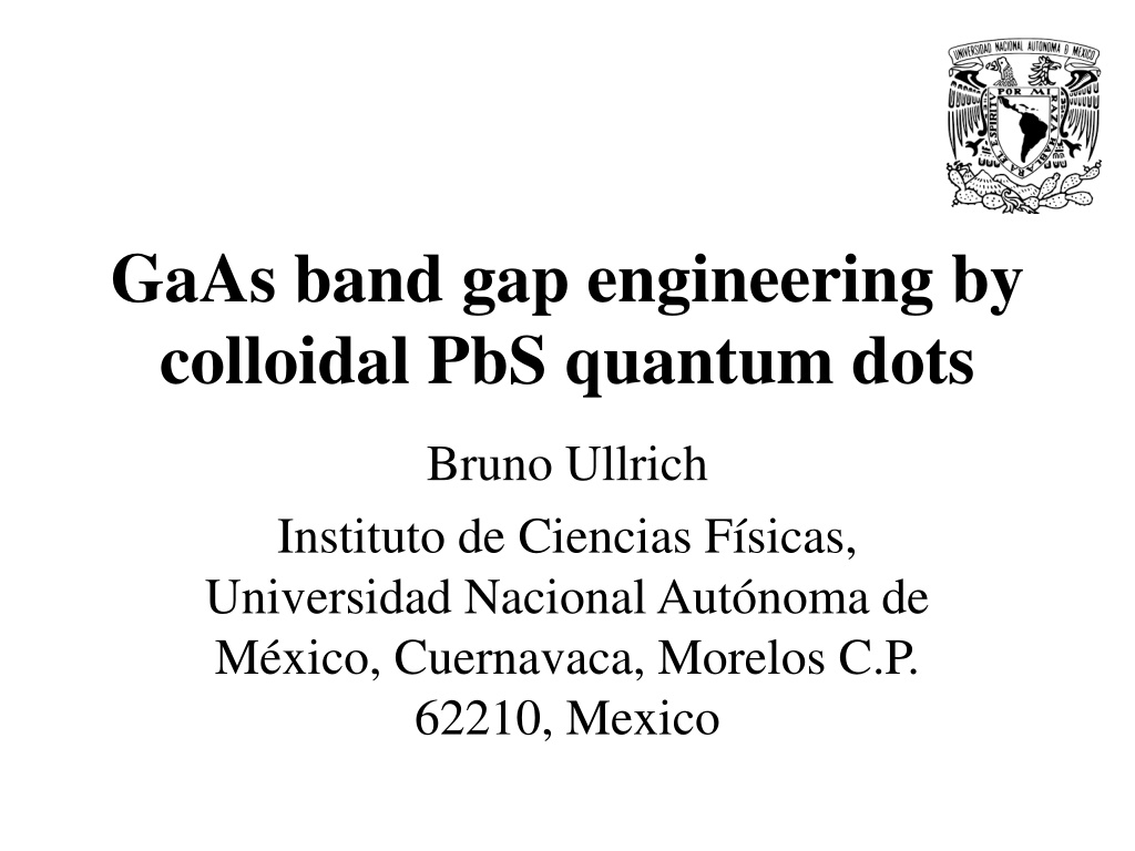
http://t1.gstatic.com/images?q=tbn:ANd9GcQDw2TrnicDQS4scJ1_ScuG4f05uVFuHsg6vVeWPCVMskM8ee9pTwhttp://t1.gstatic.com/images?q=tbn:ANd9GcQDw2TrnicDQS4scJ1_ScuG4f05uVFuHsg6vVeWPCVMskM8ee9pTw GaAs band gap engineering by colloidal PbS quantum dots Bruno Ullrich Instituto de Ciencias F sicas, Universidad Nacional Aut noma de M xico, Cuernavaca, Morelos C.P. 62210, Mexico
Acknowledgements Joanna Wang (WPAFB) Akhilesh Singh (UNAM) Puspendu Barik (UNAM) DGAPA-UNAM PAPIIT project TB100213-RR170213 (PI Bruno Ullrich)
Motivation Work in 2009 showed that PbS quantum dots (QDs) notably alter the emission of GaAs Tailored photonic applications? Ullrich et al., J. Appl. Phys. 108, 013525 (2010)
Presentations outline Essentially, two points will be covered: a) Optical properties of colloidal PbS QDs on GaAs b) Absorption edge engineering of GaAs with PbS QDs
Sample preparation Oleic acid capped PbS QDs are dispersed on GaAs either by a supercritical CO2method*)or by spin coating. *)Wang et al., Mat. Chem. Phys. 141, 195 (2013).
Why PbS, why GaAs? PbS possesses a large Bohr radius ( 20 nm). Emission covers the attractive range for optical fibers GaAs is fast and meanwhile a main player in optoelectronics
SEM image of a typical sample Particle size: 2.0 0.4 nm 20 nm
We are dealing with a size-hybrid Sample can be considered to a certain extend as free standing (regularly arranged) energy confinement potentials with similarities to superlattices. Indeed, electronic states of the QDs are coupled via tunneling.
Photoluminescence 250 120 W/cm2 90 W/cm2 72 W/cm2 60 W/cm2 48 W/cm2 30 W/cm2 18 W/cm2 12 W/cm2 6 W/cm2 5 K PL intensity (arb. units) 200 150 100 50 0 0.9 1.0 1.1 1.2 1.3 1.4 Energy (eV)
Photo-doping 1.180 1.175 EPL (eV) 1.170 1.165 1.160 1.155 0 20 40 60 80 100 120 140 Iex (W/cm2)
Burstein-Moss effect Doping by excited charge carriers increases the QD band gap Generation of at least one electron-hole pair per QD Reversible band gap alteration proportional to Iex2/3 Ullrich et al., J. Appl. Phys. 115, 233503 (2014)
Transmittance Transmittance (normalized) 300 K 4 200 K 3 100 K 2 10 K 1 GaAs PbS/GaAs 0 1.0 1.1 1.2 Energy (eV) 1.3 1.4 1.5 1.6
Absorption edge manipulation 1.2 Eg 1.0 TR (normalized) GaAs 0.8 0.6 PbS/GaAs 0.4 RT 10 K 0.2 0.0 1.0 1.1 1.2 Energy (eV) 1.3 1.4 1.5 1.6
Slope of the edge -0.30 -0.40 GaAs Normalized slope (1/eV) -0.50 -0.60 -0.70 PbS/GaAs -0.80 -0.90 -1.00 -1.10 0 50 100 Temperature (K) 150 200 250 300 350
Band gap shift 0 -10 3.0 nm QDs (Spin-coating) RT -20 dTR/dE (1/ev) -30 -40 2.0 nm QDs (CO2) -50 -60 SI-GaAs PbS/GaAs -70 -80 1.35 1.36 1.37 1.38 1.39 1.40 1.41 1.42 Energy (eV)
?Reasons? Charge transfer (Urbach tail alteration) Superposition of absorption spectra Interfacial impurities Vibronic mode manipulation Influence of preparation method and doping of the substrate (currently ongoing studies) Change of reflectance
Conclusion and future QDs alter the optical properties of the host Concentration on the emission properties for technological applications (emission from the interface?) Possible influence of the QD size on the optical properties of the host Formation of opto-electronically active junctions
Thank you! bruno@fis.unam.mx http://t1.gstatic.com/images?q=tbn:ANd9GcQDw2TrnicDQS4scJ1_ScuG4f05uVFuHsg6vVeWPCVMskM8ee9pTw