Electron Beam Generation and Cathode Research at HERACLES Facility
Research at the HERACLES facility focuses on electron beam generation and cathode development for high-current applications. Photocathodes play a crucial role in providing low energy spread beams required for processes like FEL-lasing. GaAs emerges as a promising candidate for spin-polarized electron beams due to its charge lifetime and high polarization potential. Ongoing efforts aim to enhance quantum efficiency and average current capabilities for various applications.

Download Presentation

Please find below an Image/Link to download the presentation.
The content on the website is provided AS IS for your information and personal use only. It may not be sold, licensed, or shared on other websites without obtaining consent from the author. Download presentation by click this link. If you encounter any issues during the download, it is possible that the publisher has removed the file from their server.
E N D
Presentation Transcript
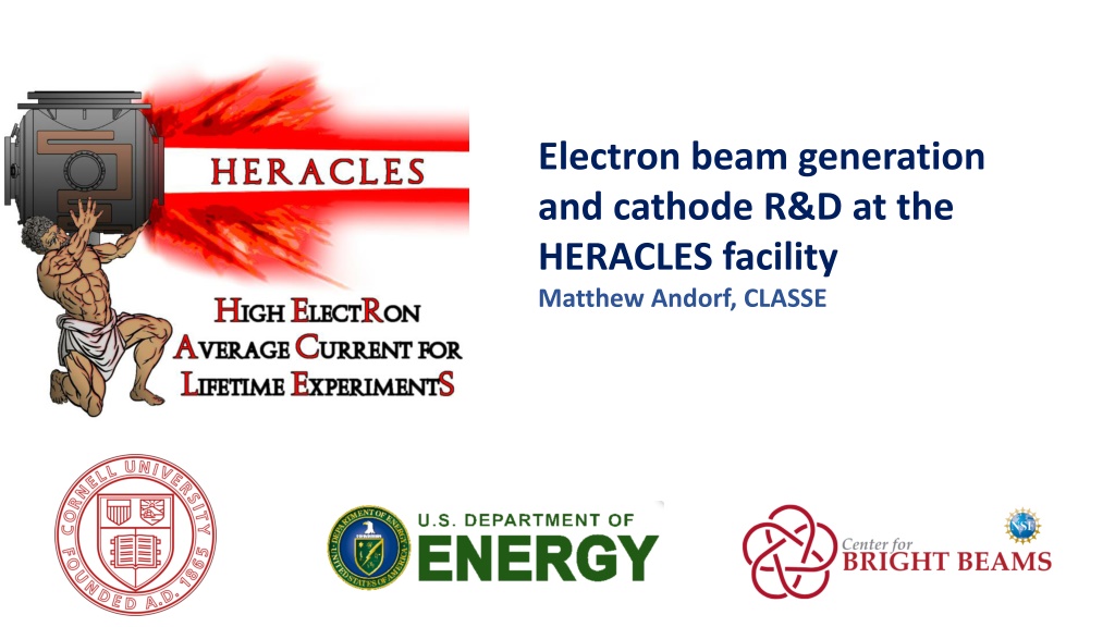
Electron beam generation and cathode R&D at the HERACLES facility Matthew Andorf, CLASSE
HERACLES TEAM In collaboration with Jai Kwan Bae (Former student) Luca Cultrera (now @ BNL) Jared Maxson Ivan Bazarov Adam Bartnik Alice Galdi (now @U. of Salerno) Sam Levenson (Graduate student)
Photocathodes for High Current applications For high brightness, photocathodes are ideal. They provide low transverse and longitudinal energy spreads Low emittance beams enable the FEL-lasing process SHC requires, a high charge bright beam with low energy spread ERL-FEL based UV lithography~ 10 mA average current For high current operation, we require a relatively high Quantum Efficiency For visible light photons, a 1% QE cathode yields ~4 mA per 1 W of laser power Metal cathodes provide QE s several orders of magnitude too small. Must use semiconductor-based cathodes! Cornell has a long history of high current photocathode development. Current record holder for highest average current from a photoinjector, 65 ma! Electron based, strong hadron cooling with an ERL needs 100 mA! Alkali-antimonides are great for these applications
Photocathodes for High Current Spin-Polarized electrons Many future facilities want spin-polarized electrons at high average currents Only candidate cathode for the job: GaAs! Charge lifetime: The amount of current extracted before the QE degrades by 1/e 1000 C is state of the art 6 hours at 50 ma! PEPPo
Pierce et al, The GaAs Spin Polarized Electron Source (1980) GaAs photocathodes for spin-polarized electron beams 0.34 eV spin-orbit splitting in the valance band: 4-fold degeneracy in p3/2 2-fold degeneracy in p1/2 Optical selection rules require m=+/- 1 for right/left-handed circularly polarized light Max polarization occurs with excitation at the bandgap where emission from p3/2 >> emission from p1/2 Theoretical max value of 50% for Bulk GaAs Straining GaAs breaks the p3/2 degeneracy theoretically allowing 100% polarization Bae et al, Rugged Spin Polarized Electron Source Based on Negative Electron Affinity GaAs photocathode with Robust Cs2Te coating (2018)
Negative Electron Affinity activation For the highest QE, GaAs are activated to Negative Electron Affinity (NEA) NEA means the bulk conduction band minimum is larger than the vacuum level NEA is typically achieved by depositing a monolayer of Cs- Oxidant onto the GaAs surface can be done by: Co-deposition: Cs is deposited until QE peaks, at which point an oxidant is leaked while Cs source remains on Yo-yo method: the cathode is over cesiated at which point the cesium source turns off. It is then exposed to an oxidant until the QE peaks, the oxidant is then turned off and cesium source back on. The cycle is repeated numerous times. Either O2 and NF3 can be used for an oxidant Problem: A monolayer is a fragile thing! Chemical poisoning: Interaction with residual gas Ion back bombardment: residual gas is ionized and accelerated towards the cathode
The Mother Chamber Mom, your love is a mystery: How can you do it all? You re always there with the perfect fix For my problems, big and small ..
The growth chamber Cs,Sb,Te,Rb sources+O2 leak valve, thermally regulated with pneumatic valve control Quartz microbalance (QMB) for deposition monitoring Substrate heater
The Auger chamber Auger Electron Spectroscopy-To characterize surface chemistry Low Energy Electron Diffraction-Chararacterize surface crystallinity Cs, O2 leak valve. Insulated, bias-able cathode holder
The TE meter 10 kV electron gun Microchannel plate for beam imaging Measure Mean Transverse Energy (MTE)
Mott polarimeter 20 keV gun + einzel lens beamline Tungsten scattering target Measure spin-polarization
GaAs with Cs3Sb as a robust NEA activation layer NEA GaAs can be generated by forming a heterojunction at the surface with another semiconductor (activation layer) subject to two criteria: 1. In the activation layer, the gap from the fermi level to vacuum should be smallerthan GaAs s bandgap (~1.4 eV). 2. So that photoemission does not occur from activation layer, its bandgap should be largerthan GaAs s. This criteria can be violated if the activation layer is sufficiently thin The above suggest using p-doped GaAs with an intrinsic semiconductor with a small electron affinity for the activation layer Cs3Sb fits this description Known to be less sensitive to chemical poisoning As a photoemitter, it can sustain 10 s of mA beam current for weeks (alkali-antimonide!) This indicates Cs3Sbmay be a very robust activation layer! intrinsic? p-type
GaAs with Cs3Sb as a robust NEA activation layer (recipes) Various activation recipes were tried and compared with Cs-O2 activation: All methods achieved NEA Overall, Cs-O2 produced the highest QE while Cs-Sb had the worse Including O2 in the activation improved QE of Sb containing recipes The QE was monitored over time to determine robustness All Sb activations outperformed pure Cs-O2 and pure Cs-Sb had the longest lifetime. Co-deposition of Cs-Sb-O finds a happy middle ground 10x Improved lifetime over Cs-O activation. 10x improved QE over Cs-Sb activation Bae et al, Improved lifetime of a high spin polarization superlattice photocathode (2020)
GaAs with Cs3Sb as a robust NEA activation layerTrade offs Cs-O-Sb co-deposition recipe was further refined through scanning the Sb layer thickness: QE and electron spin-polarization decrease with Sb layer thickness 0.12 nm layer results in only a small QE decrease while preserving max spin-polarization! Cultrera et al, Long lifetime polarized electron beam production from negative electron affinity GaAs activated with Sb-Cs-O: Trade-offs between efficiency, spin polarization, and lifetime (2020)
Ion back bombardment An electron beam can ionize residual gas which will be positively charged Ions will be accelerated towards the cathode and cause damage So far, results have been in growth chamber Low current (1-100 nA) Low voltage (-18 V) Main source of degradation comes from vacuum poisoning In a high voltage DC gun, induced damage from ion back bombardment is more severe Lower energy ions can sputter off activation layer High energy ions damage GaAs crystal structure Operation at high voltage and current is critical to testing efficacy of alternative activation layers!
Reducing beamline ions Although ionization cross-section at high energy (>100 keV) is small, a significant number of ions are generated outside the gun: Vacuum tends to be poorer in the beamlines Out gassing from beam loss Beamline is much longer than cathode/anode gap Ions can migrate from beamline into cathode/anode gap and be accelerated Biased anode can reduce migration JLAB, 2 kV bias, 22% increase in charge lifetime for GaAs Cornell developed clearing electrodes for high current running Required voltage predicted by electron beam size No reported lifetime changes but substantial reduction in beam trips
Grames et al. Charge and fluence lifetime measurements of a dc high voltage GaAs photogun at high average current(2011) Off centered cathode Transverse electric field inside the gun provides focusing towards the electrostatic center (EC) If the cathode active area is positioned off axis, away from the EC, the total number of ions striking the cathode is reduced, increasing operational lifetime. Can not eliminate ion back bombardment completely Ions generated near the cathode will still strike the active area. Smaller active reduces stray beam, further increasing lifetime. Puck used in HERACLES for GaAs running
The HERACLES beamline A beamline dedicated to the study of high current beam running: Former CU-ERL gun 200kV @ 10 mA Ion clearing electrodes 75 kW beam dump EPICS based control system Attached storage system: QE mapping, Cs-O activation
Beamline and Diagnostic details Solenoid scan characterizes cathode MTE Thermal couples register beam induced temperature rise at the dump Beamline 2 Solenoids, 3 corrector pairs (hor/vert) 2 clearing electrodes 3 screens, 1 quad detector 1 Faraday cup EMS system not implemented 3 Beam screens ensure clean beam transport from cathode to dump
Laser Setup The Ar ion laser has been refurbished and now can operated with tunable wavelength in the visible and UV. 5 W in the visible (ML) 2 W in the UV (ML)
July 17th, 2020 HERACLES commissioning low current First beam in the summer of 2020 Gun processed up to 200 keV Beam-based alignment of Electrostatic center to solenoid 1 Clean transport of beam from cathode to final view screen Mu metal, degaussing Magnet calibrations Angular kick vs current Larmor rotation
HERACLES high current demonstration Cs3Sb cathode on stainless steel puck 10 mA max current, limited by radiation trips 8 mA constant current for 3 + hours with no significant change in cathode QE Ready for cathode lifetime studies!
Cs-Sb-O activated GaAs cathode in HERACLES Goal Compare the charge lifetimes of Cs-Sb-O vs Cs-O activated GaAs. Sample Preparation: Cs-O:GaAs activated with co-deposition in a chamber attached to the rear of HERACLES. Lifetime measurements performed within hours of activation Cs-O-Sb:GaAs Activated in Mother chamber and transported via a vacuum suitcase to HERACLES ~24 hours between activation and lifetime measurement Run Conditions 1 mA beam current held constant for 2-3 hours 488 nm drive laser. QE map at 532 and 780 nm Typical vacuum pressure in the low e-10 s during run
Cs-Sb-O activated GaAs cathode in HERACLES (results) We did not see an improvement in the charge lifetime at 488 nm Pre/post run comparisons of QE indicate lifetime at 780 nm may have improved. Relative QE change smaller for Cs-Sb- O samples Cs-Sb-O had lower QE s We observed roughly a factor of 3 reduction in the QE between activation in the Mother chamber and beginning the run. Required laser power a factor of 4-10 higher The story is not over! New growth chamber on HERACLES to support Cs-Sb-O activation 780 nm drive laser Cs-Sb-O Cs-O
Summary GaAs is currently the only viable candidate for high current spin polarized production NEA activation is fragile, making the charge lifetime low compared to alkali-antimonides Cs-Sb-O activation improves GaAs lifetime in growth chambers No improvement of lifetime was observed with operation at 488 nm Some indirect evidence for improved lifetime at 780 nm Future work Lifetime studies performed at the 780 nm Upgraded growth chamber on HERACLES to allow for Cs-Sb-O testing with transporting
Analysis of QE degradation at high current Damage is caused by ion back bombardment, but how exactly? The ions can either: Sputter off the NEA activation layer Damage the bulk crystal structure Multiple GaAs samples ran in the CEBAF and IR-VUV FEL guns (JLAB) were studied after operation1 On two bulk GaAs samples: Rutherford Backscattering Spectrometry (RBS) showed no evidence of crystal damage. Secondary Ion Mass Spectrometry (SIMS) did not indicate hydrogen ion implantation On SL samples: SIMS did show ion implantation that correlated with use AND location on the sample 1V. Shutthanandan et al. PRAB 15, 063501 (2012)
Analysis of QE degradation at high current Damage is caused by ion back bombardment, but how exactly? The ions can either: Sputter off the NEA activation layer Damage the bulk crystal structure Multiple GaAs samples ran in the CEBAF and IR-VUV FEL guns (JLAB) were studied after operation1 On two bulk GaAs samples: Rutherford Backscattering Spectrometry (RBS) showed no evidence of crystal damage. Secondary Ion Mass Spectrometry (SIMS) did not indicate hydrogen ion implantation On SL samples: SIMS did show ion implantation that correlated with use AND location on the sample 1V. Shutthanandan et al. PRAB 15, 063501 (2012)
Analysis of QE degradation at high current Damage is caused by ion back bombardment, but how exactly? The ions can either: Sputter off the NEA activation layer Damage the bulk crystal structure Multiple GaAs samples ran in the CEBAF and IR-VUV FEL guns (JLAB) were studied after operation1 On two bulk GaAs samples: Rutherford Backscattering Spectrometry (RBS) showed no evidence of crystal damage. Secondary Ion Mass Spectrometry (SIMS) did not indicate hydrogen ion implantation On SL samples: SIMS did show ion implantation that correlated with use AND location on the sample 1V. Shutthanandan et al. PRAB 15, 063501 (2012)
Ion Implantation into GaAs Hydrogen ions implanted at 100 and 10000 eV for 3 different cleave planes Hypothesized 110 s smaller atomic density would support the most channeling and thus, be less damaged. QE measured as a function of heat cycles Low energy implantation resulted in QE loss that was recoverable Interstitial defects High energy resulted in some permanent loss Knock out vacancy W. Liu et al, PRAB 19, 103402 (2016)
Ion Back Bombardment in RF guns Ions are heavy enough such that over one period of acceleration, they do not travel the length of a cavity cell The ponderomotive effect causes the ions to move from strong field regions to weaker field regions In general away from the cathode Eliminates high energy bombardment (<9 keV for 700 keV gun) 1J.W. Lewellen Ion tracking in photocathode RF guns 2 Ji Qiang Particle in Cell Monte Carlo simulation of ion back bombardment in a high average current RF photo-gun