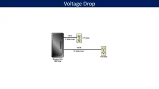
Understanding Voltage Divider Biasing in Transistors
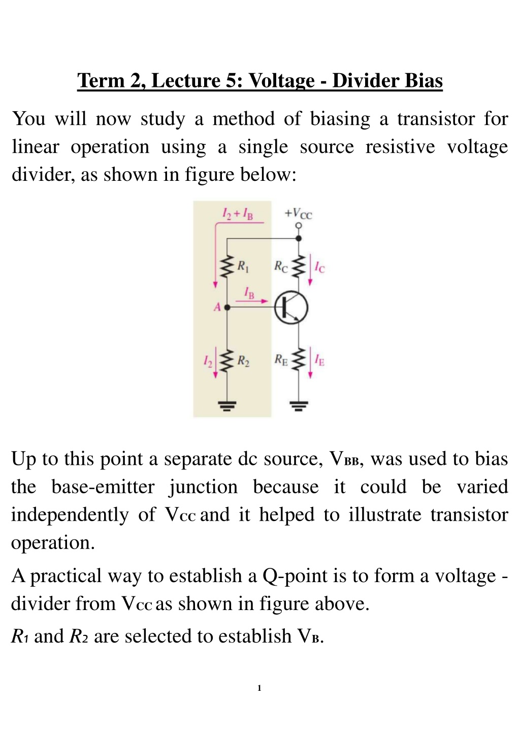
Term 2, Lecture 5: Voltage - Divider Bias
You will now study a method of biasing a transistor for
linear operation using a single source resistive voltage
divider, as shown in figure below:
Up to this point a separate dc source, V
BB
, was used to bias
the base-emitter junction because it could be varied
independently of V
CC
and it helped to illustrate transistor
operation.
A practical way to establish a Q-point is to form a voltage -
divider from V
CC
as shown in figure above.
R
1
and
R
2
are selected to establish V
B
.
1
Generally, voltage-divider bias circuits are designed so that
the base current is much smaller than the current (I
2
)
through
R
2
in Figure above. In this case, the voltage-
divider circuit is very straightforward to analyze
because
the loading effect of the base current can be ignored
. A
voltage divider in which the base current is small
compared to the current in R
2
is said to be a
stiff voltage
divider
because the base voltage is relatively independent
of different transistors and temperature effects.
If the divider is stiff,
Ib
is small compared to I
2
. Then,
2
Example:
3
Ideally, a voltage-divider circuit is stiff
, which means
that the transistor does not appear as a significant load. All
circuit design involves trade-offs; and one trade-off is that
stiff voltage dividers require smaller resistors, which are
not always desirable because of potential loading effects on
other circuits and added power requirements. If the circuit
designer wanted to raise the input resistance, the divider
may not be stiff; and more detailed analysis is required to
calculate circuit parameters. To determine if the divider is
stiff, you need to examine the dc input resistance looking
in at the base as shown in Figure below:
4
Loading Effects of Voltage-Divider Bias
(
1
)
D
C
I
n
p
u
t
R
e
s
i
s
t
a
n
c
e
a
t
t
h
e
T
r
a
n
s
i
s
t
o
r
B
a
s
e
.
5
6
2) Stability of Voltage - Divider Bias
7
8
Review Questions:
1. If the voltage at the base of a transistor is 5 V and the
base current is 5 µA, what is the dc input resistance at
the base?
2. If a transistor has a dc beta of 190,
V
b
= 2 V, and
I
e
=
2
mA, what is the dc input resistance at the base?
3. What bias voltage is developed at the base of a
transistor if both resistors in a stiff voltage divider are
equal and
V
CC
= 10 V.
4. What are two advantages of voltage-divider bias?
5
.
W
h
a
t
a
r
e
t
h
e
c
o
n
d
i
t
i
o
n
s
f
o
r
s
t
i
f
f
a
n
d
n
o
t
s
t
i
f
f
v
o
l
t
a
g
e
–
d
i
v
i
d
e
r
b
i
a
s
c
i
r
c
u
i
t
?
G
i
v
e
t
h
e
e
q
u
a
t
i
o
n
s
o
f
V
B
.
6. With the stability analysis of not stiff voltage - divider
bias circuit by using Thevenin’s theorem, give the
equation of emitter current.
9
Study how to bias a transistor for linear operation using a resistive voltage divider connected to a single source. Learn the design principles, loading effects, stability considerations, and how to calculate key parameters for a successful voltage divider bias circuit.

Download Presentation

Please find below an Image/Link to download the presentation.
The content on the website is provided AS IS for your information and personal use only. It may not be sold, licensed, or shared on other websites without obtaining consent from the author. Download presentation by click this link. If you encounter any issues during the download, it is possible that the publisher has removed the file from their server.
E N D
Presentation Transcript
Term 2, Lecture 5: Voltage - Divider Bias You will now study a method of biasing a transistor for linear operation using a single source resistive voltage divider, as shown in figure below: Up to this point a separate dc source, VBB, was used to bias the base-emitter junction because it could be varied independently of VCC and it helped to illustrate transistor operation. A practical way to establish a Q-point is to form a voltage - divider from VCC as shown in figure above. R1 and R2 are selected to establish VB. 1
Generally, voltage-divider bias circuits are designed so that the base current is much smaller than the current (I2) through R2 in Figure above. In this case, the voltage- divider circuit is very straightforward to analyze because the loading effect of the base current can be ignored. A voltage divider in which the base current is small compared to the current in R2 is said to be a stiff voltage divider because the base voltage is relatively independent of different transistors and temperature effects. If the divider is stiff, IB is small compared to I2. Then, 2
Example: 3
Ideally, a voltage-divider circuit is stiff, which means that the transistor does not appear as a significant load. All circuit design involves trade-offs; and one trade-off is that stiff voltage dividers require smaller resistors, which are not always desirable because of potential loading effects on other circuits and added power requirements. If the circuit designer wanted to raise the input resistance, the divider may not be stiff; and more detailed analysis is required to calculate circuit parameters. To determine if the divider is stiff, you need to examine the dc input resistance looking in at the base as shown in Figure below: 4
Loading Effects of Voltage-Divider Bias (1) DC Input Resistance at the Transistor Base. 5
Review Questions: 1. If the voltage at the base of a transistor is 5 V and the base current is 5 A, what is the dc input resistance at the base? 2. If a transistor has a dc beta of 190, VB= 2 V, and IE= 2 mA, what is the dc input resistance at the base? 3. What bias voltage is developed at the base of a transistor if both resistors in a stiff voltage divider are equal and VCC = 10 V. 4. What are two advantages of voltage-divider bias? 5. What are the conditions for stiff and not stiff voltage divider bias circuit? Give the equations of VB. 6. With the stability analysis of not stiff voltage - divider bias circuit by using Thevenin s theorem, give the equation of emitter current. 9


 Stability of Voltage - Divider Bias")