Understanding Zener Diodes and Breakdown Characteristics
Zener diodes play a crucial role in electronic circuits by allowing current flow in both forward and reverse biased conditions. When reverse biased voltage is applied, zener diodes exhibit a unique behavior called breakdown, where a sudden rise in current occurs leading to zener voltage and zener current. These specialized devices are designed to operate in the breakdown region without damage, offering a wide range of applications due to their specific characteristics and voltage regulation capabilities.
Download Presentation

Please find below an Image/Link to download the presentation.
The content on the website is provided AS IS for your information and personal use only. It may not be sold, licensed, or shared on other websites without obtaining consent from the author. Download presentation by click this link. If you encounter any issues during the download, it is possible that the publisher has removed the file from their server.
E N D
Presentation Transcript
DIODE DIODE BREAKDOWN BREAKDOWN
Zener diode A normal p-n junction diode allows electric current only in forward biased condition. When forward biased voltage is applied to the p-n junction diode, it allows large amount of electric current. Hence, a forward biased p-n junction diode offer only a small resistance to the electric current.
When reverse biased voltage is applied to the p-n junction diode, it blocks large amount of electric current. Hence, a reverse biased p-n junction diode offer large resistance to the electric current.
If reverse biased voltage applied to the p-n junction diode is highly increased, a sudden rise in current occurs. At this point, a small increase in voltage will rapidly increases the electric current. This sudden rise in electric current causes a junction breakdown called zener or avalanche breakdown. The voltage at which breakdown occurs is called zener voltage and the sudden increase in current is called zener current.
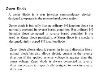
A normal p-n junction diode does not operate in breakdown region because the excess current permanently damages the diode. A zener diode is a special type of device designed to operate in the reverse breakdown region. Zener diodes acts like normal p-n junction diodes under forward biased condition (it allows large amount of electric current under forward biased voltage). Also, allows electric current in the reverse direction if the applied reverse voltage is greater than the zener voltage. Thus, it is always connected in reverse direction because designed to work in reverse direction. it is specifically
The zener breakdown voltage of the zener diode is depends on the amount of doping applied. If the diode is heavily doped, zener breakdown occurs at low reverse voltages. On the other hand, if the diode is lightly doped, the zener breakdown occurs at high reverse voltages. Zener diode is heavily doped than the normal p-n junction diode. Hence, it has very thin depletion region. Therefore, zener diodes allow more electric current than the normal p-n junction diodes. Zener diodes are available with zener voltages in the range of 1.8V to 400V.
Symbol of zener diode The symbol of zener diode is shown in the following figure : Zener cathode and anode. The symbol of zener diode is similar to the normal p-n junction diode, but with bend edges on the vertical bar diode consists of two terminals:
Advantages of zener diode Power dissipation capacity is very high High accuracy Small size and Low cost Applications of zener diode It is normally used as voltage reference. Zener diodes are used in voltage stabilizers or shunt regulators. Zener diodes are used in switching operations. Zener diodes are used in clipping and clamping circuits.
Diode Breakdown Diodes only allow a considerable current to flow when they are connected in forward bias. Therefore, they can be used to ensure that current in a circuit flows along a given direction. For instance, diodes can be used to convert alternating current to direct current.
However, a large reverse voltage can cause reverse currents to flow. This is referred to as breakdown, and can take place either as Zener breakdown or as avalanche breakdown. The differences between the two types of breakdown are outlined below.
Avalanche breakdown The avalanche breakdown occurs in both normal and zener diodes at high reverse voltage. When high reverse voltage is applied to the p-n junction diode, the free electrons gains large amount of energy and accelerated to greater velocities. These free electrons moving at high speed will collides with the atoms and knock off more electrons.
These electrons are again accelerated and collide with other atoms. Because of this continuous collision with the atoms, a large number of free electrons are generated. As a result, electric current in the diode increases rapidly. This sudden increase in electric current may permanently destroys the normal diode
However, zener diodes may not be destroyed because they are carefully designed to operate in avalanche breakdown region. Avalanche breakdown occurs in zener diodes with zener voltage (Vz) greater than 6V.
In terms of energy bands, the incoming charge carrier s kinetic energy must be larger than the energy gap between conduction and valence bands for impact ionization to take place. Then, once the collision takes place and the electron-hole pair is formed, this electron and the hole are essentially in the conduction and valance bands respectively.
For most diodes, avalanche breakdown is the dominant effect which is determined by: 1- The material used to construct the junction. 2- The level of doping.
Zener breakdown In Zener breakdown, electrons tunnel from the valence band of the p side to the conduction band on the n side. In classical physics, electrons should not have been able to cross over in this way. The probability for an electron to tunnel across is higher when: 1- the space charge region is narrower 2- the electric field is larger.
Typically, Zener breakdown occurs when materials used to construct the p n junction are heavily doped. In these junctions, due to heavy doping, the space charge region is quite narrow even when the junction is under reverse bias. When reverse biased voltage applied to the diode reaches close to zener voltage, the electric field in the depletion region is strong enough to pull electrons from their valence electrons which gains sufficient energy from the strong electric field of depletion region will breaks bonding with the parent atom and become free electrons. These free electrons carry electric current from one place to another place. At zener breakdown region, a small increase in voltage will rapidly increases the electric current valence band. The
Difference Between Zener and Avalanche Breakdown Zener breakdown occurs when the doping levels are high, and involves electrons tunnelling from the valence band of the p side to the conduction band on the n side. Avalanche breakdown occurs when charge carriers which are accelerated by the electric field gain enough kinetic energy such that, when they collide with lattice atoms, they ionise the lattice atoms to produce electron-hole pairs. These pairs, in turn, cause further ionizations, leading to an avalanche effect Zener breakdown occurs at low reverse voltage whereas avalanche breakdown occurs at high reverse voltage.
END END


