Basic Concepts of Microscopy for Materials Study

Microscopy plays a crucial role in examining the structural elements and defects influencing material properties. This involves studying microscopic features like grain size and shape using optical, electron, and scanning probe microscopes. Microstructural examinations help understand property-structure relationships, predict material properties, design new alloys, verify heat treatments, and determine mechanical fracture modes. Optical microscopy is commonly used for opaque materials, requiring meticulous surface preparation to reveal the microstructure details.

Download Presentation

Please find below an Image/Link to download the presentation.
The content on the website is provided AS IS for your information and personal use only. It may not be sold, licensed, or shared on other websites without obtaining consent from the author. Download presentation by click this link. If you encounter any issues during the download, it is possible that the publisher has removed the file from their server.
E N D
Presentation Transcript
4.1 BASIC CONCEPTS OF MICROSCOPY On occasion it is necessary or desirable to examine the structural elements and defects that influence the properties of materials. Some structural elements are of macroscopic dimensions; that is, they are large enough to be observed with the unaided eye. For example, the shape and average size or diameter of the grains for a polycrystalline specimen are important structural characteristics. Macroscopic grains are often evident on aluminum streetlight posts and also on highway guardrails. Relatively large grains having different textures are clearly visible on the surface of the sectioned copper ingot shown in Figure 4.1. However, in most materials the constituent grains are of microscopic dimensions, having diameters that may be on the order of microns,10 and their details must be investigated using some type of microscope. Grain size and shape are only two features of what is termed the microstructure; these and other microstructural characteristics are discussed in subsequent chapters. Optical, electron, and scanning probe microscopes are commonly used in microscopy. These instruments aid in investigations of the microstructural features of all material types. Some of these techniques employ photographic equipment in conjunction with the microscope; the photograph on which the image is recorded is called a photomicrograph. In addition, many microstructural images are computer generated and/or enhanced.
Microscopic examination is an extremely useful tool in the study and characterization of materials. Several important applications of microstructural examinations are as follows: to ensure that the associations between the properties and structure (and defects) are properly understood, to predict the properties of materials once these relationships have been established, to design alloys with new property combinations, to determine whether a material has been correctly heat-treated, and to ascertain the mode of mechanical fracture. Several techniques that are commonly used in such investigations are discussed next. Figure 4.1 Cross-section of a cylindrical copper ingot. The small, needle-shape grains may be observed, which extend from the center radially outward.
4.2 MICROSCOPIC TECHNIQUES Optical Microscopy With optical microscopy, the light microscope is used to study the microstructure; optical and illumination systems are its basic elements. For materials that are opaque to visible light (all metals and many ceramics and polymers), only the surface is subject to observation, and the light microscope must be used in a reflecting mode. Contrasts in the image produced result from differences in reflectivity of the various regions of the microstructure. Investigations of this type are often termed metallographic because metals were first examined using this technique. Normally, careful and meticulous surface preparations are necessary to reveal the important details of the microstructure. The specimen surface must first be ground and polished to a smooth and mirror-like finish. This is accomplished by using successively finer abrasive papers and powders. The microstructure is revealed by a surface treatment using an appropriate chemical reagent in a procedure termed etching. The chemical reactivity of the grains of some single- phase materials depends on crystallographic orientation. Consequently, in a polycrystalline specimen, etching characteristics vary from grain to grain. Figure 4.2b shows how normally incident light is reflected by three etched surface grains, each having a different orientation. Figure 4.2a depicts the surface structure as it might appear when viewed with the microscope; the luster or texture of each grain depends on its reflectance properties. A photomicrograph of a polycrystalline specimen exhibiting these characteristics is shown in Figure 4.2c.
Figure 4.2 (a) Polished and etched grains as they might appear when viewed with an optical microscope. (b) Section taken through these grains showing how the etching characteristics and resulting surface texture vary from grain to grain because of differences in crystallographic orientation. (c) Photomicrograph of a polycrystalline brass specimen, X60.
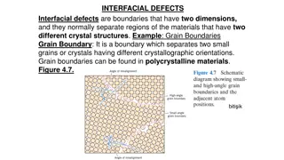
Figure 4.3 (a) Section of a grain boundary and its surface groove produced by etching; the light reflection characteristics in the vicinity of the groove are also shown. (b) Photomicrograph of the surface of a polished and etched polycrystalline specimen of an iron chromium alloy in which the grain boundaries appear dark, X100.
Also, small grooves form along grain boundaries as a consequence of etching. Because atoms along grain boundary regions are more chemically active, they dissolve at a greater rate than those within the grains. These grooves become discernible when viewed under a microscope because they reflect light at an angle different from that of the grains themselves; this effect is displayed in Figure 4.3a. Figure 4.3b is a photomicrograph of a polycrystalline specimen in which the grain boundary grooves are clearly visible as dark lines. When the microstructure of a two-phase alloy is to be examined, an etchant is often chosen that produces a different texture for each phase so that the different phases may be distinguished from each other. Electron Microscopy The upper limit to the magnification possible with an optical microscope is approximately 2000. Consequently, some structural elements are too fine or small to permit observation using optical microscopy. Under such circumstances, the electron microscope, which is capable of much higher magnifications, may be employed. An image of the structure under investigation is formed using beams of electrons instead of light radiation. According to quantum mechanics, a high-velocity electron becomes wavelike, having a wavelength that is inversely proportional to its velocity. When accelerated across large voltages, electrons can be made to have wavelengths on the order of 0.003 nm (3 pm). High magnifications and resolving powers of these microscopes are consequences of the short wavelengths of electron beams. The electron beam is focused and the image formed with magnetic lenses; otherwise, the geometry of the microscope components is essentially the same as with optical systems. Both transmission and reflection beam modes of operation are possible for electron microscopes.
Transmission Electron Microscopy The image seen with a transmission electron microscope (TEM) is formed by an electron beam that passes through the specimen. Details of internal microstructural features are accessible to observation; contrasts in the image are produced by differences in beam scattering or diffraction produced between various elements of the microstructure or defect. Because solid materials are highly absorptive to electron beams, a specimen to be examined must be prepared in the form of a very thin foil; this ensures transmission through the specimen of an appreciable fraction of the incident beam. The transmitted beam is projected onto a fluorescent screen or a photographic film so that the image may be viewed. Magnifications approaching 1,000,000 are possible with transmission electron microscopy, which is frequently used to study dislocations. Scanning Electron Microscopy A more recent and extremely useful investigative tool is the scanning electron microscope (SEM). The surface of a specimen to be examined is scanned with an electron beam, and the reflected (or back-scattered) beam of electrons is collected and then displayed at the same scanning rate on a cathode ray tube (CRT; similar to a CRT television screen). The image on the screen, which may be photographed, represents the surface features of the specimen. The surface may or may not be polished and etched, but it must be electrically conductive; a very thin metallic surface coating must be applied to nonconductive materials. Magnifications ranging from 10 to in excess of 50,000 are possible, as are also very great depths of field. Accessory equipment permits qualitative and semi quantitative analysis of the elemental composition of very localized surface areas.
Scanning Probe Microscopy In the past two decades, the field of microscopy has experienced a revolution with the development of a new family of scanning probe microscopes. The scanning probe microscope (SPM), of which there are several varieties, differs from optical and electron microscopes in that neither light nor electrons are used to form an image. Rather, the microscope generates a topographical map, on an atomic scale, that is a representation of surface features and characteristics of the specimen being examined. Some of the features that differentiate the SPM from other microscopic techniques are as follows: Examination on the nanometer scale is possible inasmuch as magnifications as high as 109 are possible; much better resolutions are attainable than with other microscopic techniques. Three-dimensional magnified images are generated that provide topographical information about features of interest. Some SPMs may be operated in a variety of environments (e.g., vacuum, air, liquid); thus, a particular specimen may be examined in its most suitable environment. Scanning probe microscopes employ a tiny probe with a very sharp tip that is brought into very close proximity (i.e., to within on the order of a nanometer) of the specimen surface. This probe is then raster-scanned across the plane of the surface. During scanning, the probe experiences deflections perpendicular to this plane in response to electronic or other interactions between the probe and specimen surface.
Figure 4.4 (a) Bar chart showing size ranges for several structural features found in materials. (b) Bar chart showing the useful resolution ranges for four microscopic techniques discussed in this chapter, in addition to the naked eye.
to and stored in a computer, which then generates the three-dimensional surface image. These new SPMs, which allow examination of the surface of materials at the atomic and molecular level, have provided a wealth of information about a host of materials, from integrated circuit chips to biological molecules. Indeed, the advent of the SPMs has helped to usher in the era of nanomaterials materials whose properties are designed by engineering atomic and molecular structures. Figure 4.4a is a bar chart showing dimensional size ranges for several types of structures found in materials (note that the axes are scaled logarithmically). The useful dimensional resolution ranges for the several microscopic techniques discussed in this chapter(plus the naked eye) are presented in the bar chart of Figure 4.4b. (plus the naked eye) are presented in the bar chart of Figure 4.4b. For three of these techniques (SPM, TEM, and SEM), an upper resolution value is not imposed by the characteristics of the microscope and, therefore, is somewhat arbitrary and not well defined. Furthermore, by comparing Figures 4.4a and 4.4b, it is possible to decide which microscopic technique(s) is (are) best suited for examination of each of the structure types. 4.3 GRAIN-SIZE DETERMINATION The grain size is often determined when the properties of polycrystalline and single phase materials are under consideration. In this regard, it is important to realize that for each material, the constituent grains have a variety of shapes and a distribution of sizes. Grain size may be specified in terms of average or mean grain diameter, and a number of techniques have been developed to measure this parameter.


 Polished and etched grains as they might")
 Section of a grain boundary and its surface")


 Bar chart showing size ranges for several")