Understanding Interfacial Defects and Microscopy in Materials Science
Interfacial defects are boundaries separating regions with different crystal structures, like grain boundaries in polycrystalline materials. Microscopic examination distinguishes between macroscopic and microscopic dimensions, analyzed through optical and electron microscopy methods. Electron microscopes provide high-resolution imaging capabilities, such as Transmission Electron Microscopes (TEM) for thin film sample analysis and Scanning Electron Microscopes (SEM) for surface characterization.
Download Presentation

Please find below an Image/Link to download the presentation.
The content on the website is provided AS IS for your information and personal use only. It may not be sold, licensed, or shared on other websites without obtaining consent from the author. Download presentation by click this link. If you encounter any issues during the download, it is possible that the publisher has removed the file from their server.
E N D
Presentation Transcript
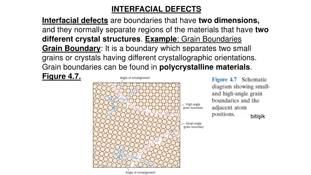
INTERFACIAL DEFECTS Interfacial defects are boundaries that have two dimensions, and they normally separate regions of the materials that have two different crystal structures. Example: Grain Boundaries Grain Boundary: It is a boundary which separates two small grains or crystals having different crystallographic orientations. Grain boundaries can be found in polycrystalline materials. Figure 4.7. biti ik
MICROSCOPIC EXAMINATION Macroscopic dimensions: They are dimensions which can be observed with the unaided eye ( plak g z). Example: Large grains on the aluminium garbage can have diameters on the order of centimeters. Microscopic dimensions: They are dimensions which are on the order of microns and can be observed with a microscope. Microstructure: It is a term which describes the microscopic grain size and shape.
MICROSCOPY Both optical and electron microscopes are commonly used in microscopy. These microscopes are used in the investigation of microstructures in materials. Photomicrograph: It is a photograph on which the image is recorded. 1. Optical Microscopy: The visible light is used as the source. Optical microscopy is used to study the surface microstructure of materials. All metals, many ceramics and polymers can be studied. Normally, careful surface preparations are necessary in order to look at a material with an optical microscope.
MICROSCOPY Example: Polishing a metal surface and etching (a nd rma) the surface with a special chemical. The minimum dimension that can be seen with an optical microscope is about 1 micrometer ( m) (1.0 10-6meters). 2. Electron Microscopy: The electrons are used as the source for electron microscopy. The electrons are focused on the sample and the image is formed with magnetic lenses. The minimum dimension that can be seen with an electron microscope is about 1 Angstrom ( ) (1.0 10-10meters).
a. Transmission Electron Microscope (TEM): TEM image is formed by an electron beam that passes through the sample. The sample must be prepared as a thin film. Magnifications of 1,000,000 is possible in TEM. TEM is usually used in the study of grain boundaries and dislocations b. Scanning Electron Microscope (SEM): The source is electrons. The surface of a sample is scanned with an electron beam. It is used in the surface characterization of materials. Magnifications of 50,000 is possible in SEM
Nitrogen Tank Sample Holder Electron Tube With Magnetic Lenses Inside ~2.5 m long Computer Data Screen Photographic Camera Box Fluorescent Screen
HOMEWORK 1.What are the Primary Interatomic Bonds? What are the differences between Ionic Bonding, Covalent Bonding and metallic Bonding? In your answer, compare them in terms of three different properties. Draw the schematic representations of ionic bonding and metallic bonding. Label all the important terms on the figures.
HOMEWORK 2. What are the definitions of the crystalline and amorphous material? What is the difference between the BCC and FCC crystal structure? Draw their crystal structures.
HOMEWORK 3.What is the difference between a vacancy and a dislocation? In your answer, please write the differences in terms of two different properties. Draw the structure of a vacancy, and define the important terms on the figure.
