Studies on Defects in ZnO Nanowires and Their Impact on Properties
In this research, various aspects of defects in ZnO nanowires are explored, including their formation through heating and ion bombardment, as well as the role of contacts. The investigation delves into the growth, control, and motivation of defects, showcasing the effects of processes like argon bombardment and heating on the properties of the nanowires. The study highlights the significance of defects on the conductivity, transport, contacts, and sensing capabilities of ZnO nanowires. Additionally, models depicting the impact of argon bombardment on nanowire defects are discussed.
Download Presentation

Please find below an Image/Link to download the presentation.
The content on the website is provided AS IS for your information and personal use only. It may not be sold, licensed, or shared on other websites without obtaining consent from the author.If you encounter any issues during the download, it is possible that the publisher has removed the file from their server.
You are allowed to download the files provided on this website for personal or commercial use, subject to the condition that they are used lawfully. All files are the property of their respective owners.
The content on the website is provided AS IS for your information and personal use only. It may not be sold, licensed, or shared on other websites without obtaining consent from the author.
E N D
Presentation Transcript
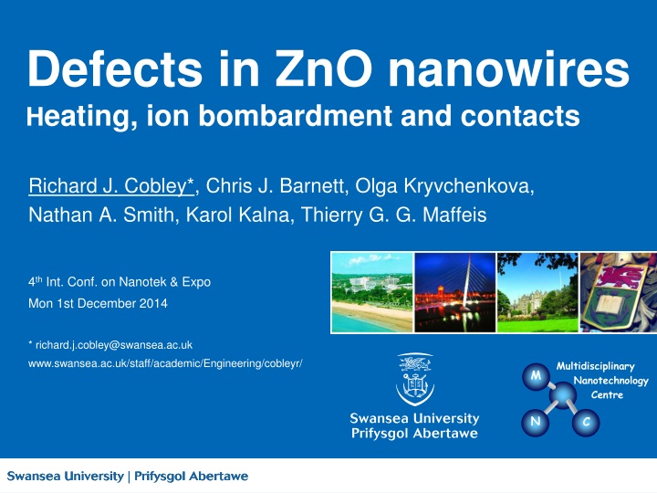
Defects in ZnO nanowires Heating, ion bombardment and contacts Richard J. Cobley*, Chris J. Barnett, Olga Kryvchenkova, Nathan A. Smith, Karol Kalna, Thierry G. G. Maffeis 4th Int. Conf. on Nanotek & Expo Mon 1st December 2014 * richard.j.cobley@swansea.ac.uk www.swansea.ac.uk/staff/academic/Engineering/cobleyr/ Multidisciplinary Nanotechnology Centre M N C
ZnO nanostructures and defects Z.L. Wang, J. Phys.: Condens. Matter 16 (2004) R829-R858 - Properties - Structures and devices - Defects Liu, J., et al, J. Phys. D: Appl. Phys., 2009. 42(9): p. 095401. 2/8
Growth, control of defects and motivation O vacancy + or ++ charge O interstitial no charge O occupying zinc site - Control and evolution of defects with argon bombardment and annealing 595 nm VO+/VO++ 520 nm Ozn 543 nm Oi - Role of defects on conductivity, transport, contacts and sensing 3/8
Effect of argon bombardment 13 5x 10 2.5 -1V +1V Normalised intensity of defect band 2 A Normalised resistance [ /m] 4 2 PL defect 3 1.5 2 23 A 1 1 0.5 0 0 0 5 5 10 10 15 15 20 20 25 25 Argon-induced current [ A] 26 A 1. Damage (PL) 3. Chemistry (XPS) 2. Ar implantation (EDS) 4. Etching? 4/8
Argon bombardment -> model of NW defects 13 5x 10 15 2.5 150 1e13 cm-2 -1V +1V Normalised intensity of defect band 10 2uA 100 Normalised resistance [ /m] 4 Current (uA) 5 2 50 PL defect 0 0 3 -1.0-0.8-0.6-0.4-0.20.0 0.2 0.4 0.6 0.8 -5 1.5 -50 2 -10 -100 -15 1 -150 1 -1 -0.5 0 0.5 1 1 Bias (V) 0.15 0.8 0.5 0 0.1 no charge 26uA 0.6 0 0 5 5 10 10 15 15 20 20 25 25 0.4 Argon-induced current [ A] 0.05 Current (uA) 0.2 0 0 0.0 0.2 0.4 0.6 0.8 -1.0 -0.8 -0.6 -0.4 -0.2 -0.05 -0.2 -0.4 -0.1 -0.6 -0.15 -0.8 -1 -0.2 -1 -0.5 0 0.5 1 1. Clean (no +defect) 3. Pitted -> sensor Bias (V) 2. PL not surface 4. Band model? 5/8
Effect of heating on hydrothermal ZnO NWs 3.5 8 3 Before 500 C 600 C 700 C 800 C Normalised intensity 2.5 6 2 1.5 log10|I| (nA) + offset 4 1 0.5 2 0 200 300 400 PL Wavelength (nm) 500 600 700 800 640 nm Ozn VO++ -> VO 0 1. 2. 3. 500 C Cleaning 600 C Donors + acceptor states present >=700C Donors reduced, acceptors -2 -4 -2 0 2 4 Gap Voltage (V) 6/8
ZnO NW role of contacts 59 nm 50 nm 47 nm 40 nm 36 nm Controlling the electrical transport properties of nanocontacts to nanowires , In preparation, AM Lord, TG Maffeis, O Kryvchenkova, RJ Cobley, K Kalna, DM Kepaptsoglou, QM Ramasse, AS Walton, MB Ward, J K ble, SP Wilks 7/8
Conclusion ZnO NWs Ohmic contacts possible with light Ar treatment, without additional defects Surface pitting with intermediate Ar, more surface but still with Ohmic contact -> better sensing? Heating alters the ratio of donors and acceptors? Growth surface defects very localised to surface can be removed by a light argon treatment PL not dominated by surface -- probing bulk of wire? In wide NWs the defect density drops towards centre -> current in a ring? Larger wires still surface sensitive? 8/8
