PCB Design Best Practices and Tips
Discover the comprehensive process of PCB design, from the initial vision to schematic capture, component placement, and route tracing using tools like Eagle PCB. Learn about various package types, general tips for layout optimization, and recommendations for placing power and ground traces effectively. Access online resources for calculating trace widths and resistances, and enhance your PCB design skills with valuable insights shared here.

Download Presentation

Please find below an Image/Link to download the presentation.
The content on the website is provided AS IS for your information and personal use only. It may not be sold, licensed, or shared on other websites without obtaining consent from the author.If you encounter any issues during the download, it is possible that the publisher has removed the file from their server.
You are allowed to download the files provided on this website for personal or commercial use, subject to the condition that they are used lawfully. All files are the property of their respective owners.
The content on the website is provided AS IS for your information and personal use only. It may not be sold, licensed, or shared on other websites without obtaining consent from the author.
E N D
Presentation Transcript
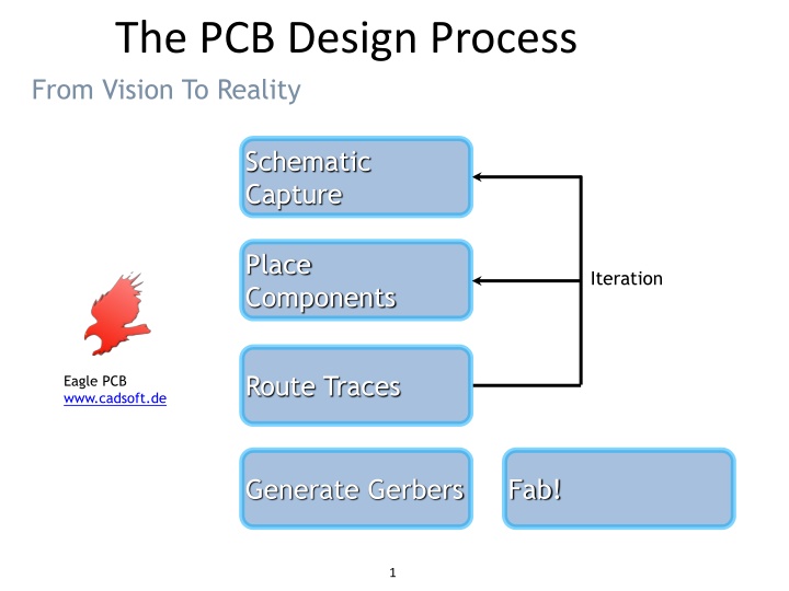
The PCB Design Process From Vision To Reality Schematic Capture Place Components Iteration Route Traces Eagle PCB www.cadsoft.de Generate Gerbers Fab! 1
EAGLE SCHEMATIC FUNCTIONS Grid adjust Cut Bus Redraw Show Wire Zoom out Information Generate board Zoom in Layers Add text Fit to design Copy Add value Print Move Add Name Open Mirror Add part Save Rotate Delete Paste Redo Group Settings Undo Select
DIL PACKAGE It is the package that allows the usage of devices with Pins and holes on the PCB SMD PACKAGE It is the package that allows the usage of Surface Mount Devices on the PCB
General tips Make important nodes accessible Give space between components Place components with the same orientation Print the layout to see if components' sizes match Exchange wiring directions between layers Select the width of lines depending on current Avoid 90 angles with traces Use the silk layer Use the schematic vs. layout comparison Create a ground plane Place bypass capacitors Consider spots of heat Tips for power circuits Keep power and control grounds separate Use an inner layer for the control ground Make power traces wider to withstand higher currents Tips for mixed-signal circuits Keep digital and analog grounds separate Protect analog grounds from noise Tips for PCB mounting Solder from small to large components Be aware of cold solder joints Use flux for easy soldering Do not trust the multimeter continuity test
Placing Power and Ground Traces When placing traces, it is always a good practice to make them as short and direct as possible. Use vias (also called feed-through holes) to move signals from one layer to the other. A via is a pad with a plated-through hole. Generally, the best strategy is to lay out a board with vertical traces on one side and horizontal traces on the other. Add via where needed to connect a horizontal trace to a vertical trace on the opposite side. A good trace width for low current digital and analog signals is 0.010 . Traces that carry significant current should be wider than signal traces. The table below gives rough guidelines of how wide to make a trace for a given amount of current. 0.010 0.3 Amps 0.015 0.4 Amps 0.020 0.7 Amps 0.025 1.0 Amps 0.050 2.0 Amps 0.100 4.0 Amps 0.150 6.0 Amps When placing a trace, it is very important to think about the space between the trace and any adjacent traces or pads. You want to make sure that there is a minimum gap of 0.007 between items, 0.010 is better. Leaving less blank space runs the risk of a short developing in the board manufacturing process. It is also necessary to leave larger gaps when working with high voltage. PCB Trace width On line calculator: http://circuitcalculator.com/wordpress/2006/01/31/pcb-trace-width-calculator/ PCB Trace Resistance On line calculator: http://circuitcalculator.com/wordpress/2006/01/24/trace-resistance-calculator
Place bypass capacitors Bypass capacitors are used to filter AC components from your constant power supply. They reduce noise, ripples and other unwanted AC signals. They do so by bypassing these AC fluctuations to ground, which gives them the name. Therefore, they are usually connected between wherever voltage we want to filter (supply voltage, reference signals, etc.) and ground. A good place to choose for these capacitors is at the power inlet to your PCB: the wires connecting the power supply to your PCB are usually long and act as antennas, collecting lots of RF signals. Another effective place is close to the ICs (as close as possible to the power and ground pins), to reduce any noise added inside your PCB. The same holds true for reference pins, or any other pin where you need a very stable voltage. The values of the capacitors depend on the frequencies of the AC components. Each capacitor has its own frequency response determined by its resistance and Equivalent Series Inductance (ESL) that is tuned to a range of frequencies. For example, to filter low frequencies you need a larger capacitor. As a rule, a capacitor of 0.1-1 F suffices for the mid-range frequencies, if you have slow fluctuations, you may choose around 1-10 F and for high-frequency noise you can use 0.001-0.1 F capacitors. You can also use any combination of bypass capacitors to remove a wider range of frequencies. For chips that drive a lot of current, you may put 10 F - 100 F capacitors to work as buffers. If the value of the capacitor allows, use monolithic ceramic capacitors because they are small and cheap.
Checking Your Work After all the traces are placed, it is best to double check the routing of every signal to verify that nothing is missing or incorrectly wired. Do this by running through your schematic, one wire at a time. Carefully follow the path of each trace on your PC layout to verify that it is the same as on your schematic. After each trace is confirmed, mark that signal on the schematic with a yellow highlighter. Inspect your layout, both top and bottom, to insure that the gap between every item (pad to pad, pad to trace, trace to trace) is 0.007 or greater. Use the Pad Information tool to determine the diameters of pads that make up a component. Check for traces that cross each other. This is easily done by inspecting a printout of each layer. Metal components such as heat sinks, crystals, switches, batteries and connectors can cause shorts if they are placed over traces on the top layer. Inspect for these shorts by placing all the metal components on a printout of the top layer. Then look for traces that run below the metal components.
IMPORTANT RULES WHILE DESIGNING 1) If it is available for you to use connectors go on 2) Always check DRC while working to know exactly where is your error 3) Always use the name and the value of any element to make your design clear and prepared well for soldering 4) Try to compress the area of your design as possible 5) Make always capacitors between higher and lower Voltage supplies 6) Make the Power signal and ground more thick in the design to be distinguished from wires of signals
Autorouter Helps engineer to correctly route the paths on the board Uses method Ripup/ Retry when there is no more further path lay down possibility disconnecting existing one Change between manual and automatic routing at any time Fully integrated with basic program
Schematic Capture Place Components Some General Tips Place Components Are your Design Rules setup correctly? Run the Design Rule Check (DRC) often. Run the Electrical Rule Check (ERC) often. Save a snapshot of your placement file.
Manufacturing Files Gerber Files Industry standard file format to describe circuits Generated by PCB design software Contains all necessary info to manufacture a circuit board (Traces, Pads, Silkscreen, etc.) Drill Files Describes the location and size of holes Zipped with Gerber files and sent to manufacturer 17
Design For auto router: Edit - > Design rules -> Sizes -> Minimum width - > 24 mils To cancel routing: Edit - > Ripup - > GO File - > Export - > Image -> Browse : File Name File - > Export - > Part list -> Browse : File Name Generate/Switch to board -> File - > CAM Processor -> File -> Open -> Job -> gerb274x.cam - > Process Job File - > CAM Processor -> File -> Open -> Job -> excellon.cam - > Process Job File -> Run ULP -> drillcfg.ulp - > OK > Save
3D visualization Recommended free application POVRay project can be seen in 3D www.povray.org/download https://www.youtube.com/watch?v=OZLU4828Rp Y https://www.youtube.com/watch?v=BUl828AW0T E
Emtron Technologies Emtron Technologies Flat No-101, B3 Wing, 1st Floor, Divyam Hights, Gilbert Hill, Shreenath Nagar, Andheri West, Mumbai-58 +91-8080181911 E-mail: emtron.tech@gmail.com, www.emtrontech.in Thank You!! 21


")