Introduction to DSP Processors and Applications

UNIT-5
Introduction to DSP
Processors
By
Srikanth.I
Assoc.Prof, ECE Dept
Methodist College of
Engineering and Technology
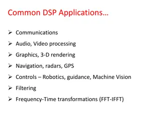
Common DSP Applications…
Communications
Audio, Video processing
Graphics, 3-D rendering
Navigation, radars, GPS
Controls – Robotics, guidance, Machine Vision
Filtering
Frequency-Time transformations (FFT-IFFT)
Common DSP Tasks…
Modulation-Demodulation, Error correction
Noise reduction, equalization, echo cancellation
Audio compression
Vector and Matrix calculations
Control algorithms
DSPs Need to Do…
Efficient repetitive numerical calculations
Maintain numeric fidelity
Provide high memory bandwidth
Streaming data
Real Time processing
DSPs Need to Minimize…
Real Time execution unpredictability
Memory use
Power consumption
Cost
Development time
What Do DSPs Have?
Specialized memory architecture (Harvard)
Specialized parallel execution units
Specialized addressing modes
Specialized instruction sets for parallelexecution
Specialized peripherals
Multiply-Accumulate (MAC)
•
Multiplication in single cycle
•
Execution time ~ 200 ns
Register
Multiplier
ALU
Accumulator
Von Neumann Architecture
Harvard Architecture…
Harvard Architecture with Dual Data Memory
Von Neumann Architecture…
Processor Core
Memory
(Code+Data)
Address bus
Data bus
1.
Fetch MAC instruction
2.
Read value of ‘x’
3.
Read value of ‘h’
4.
Multiply x, h and accumulate
5.
Write result to memory
•
4 memory access
operations
•
One multiplication
Harvard Architecture…
1.
Data and Code in
separate memory
segments
2.
Multiple address and
data buses
3.
Double memory
bandwidth
4.
Simultaneous code and
data fetch
AB1
AB2
DB1
DB2
Summary
Von Neumann
=
Shares the same data bus and the same main
memory for transfer storage of instructions and data of the
programs.
Von Neumann is better for desktop computers/high
performance computers were cost to performance ratio is
important.
Harvard
=
Uses two separate buses for the transfer of data and
instructions and two separate memories for storage of data and
instructions.
Harvard architecture is used primarily for small embedded
computers and signal processing. Commonly used within CPUs to
handle the cache.
Main differences
Cell sizes used within the main memory are same in
Von
Neumann
. However,
Harvard
allows for different cell sizes for
data/instructions making effective use of resources.
The programs in Harvard tend to be large.
Modern computers make use of
both
Harvard and Von
Neumann architecture.
The main memory is used to store both instructions and data
and they are both transferred over the data bus. However, the
CPU’s cache has Harvard architecture.
There is a separate cache memory for instructions and data.
There is also a separate data bus between these caches.
Von Neumann Architecture
Advantages
Not only data but also instructions of programs are stored within the same memory.
This makes it easier to re-program the memory.
Memory organisation is within the hands of the programmer.
Data from memory and devices is accessed in the same way.
The control unit gets data and instructions in the same way from one memory so
simplifies the design and development of the control unit.
Disadvantages
Has only one data bus shared from the transfer of data transfers and instruction fetches;
they must be scheduled because they cannot run simultaneously.
Serial instruction processing does not allow for parallel execution of programs.
Paralleled executions must be simulated later by the operating system (i.e. no pipelining)
Higher chance of corruption or error as the instructions and data are stored and
transferred in the same way so may be accidently rewritten by bugs in programs.
All memory cell sizes are the same and so can’t be different for instructions/data making
it less efficient.
Harvard Architecture
Advantages
There is less chance of corruption since data and instructions are transferred via different
buses.
2/18/2025
Embedded Computer Architecture H.
Corporaal and B. Mesman
16
VLIW characteristics
•
Multiple operations per instruction
•
One instruction per cycle issued (at most)
•
Compiler is in control
•
Only RISC like operation support
–
Short cycle times
–
Easier to compile for
•
Flexible: Can implement any FU mixture
•
Extensible / Scalable
However:
•
tight inter FU connectivity required
•
not binary compatible !!
–
(new long instruction format)
•
low code density
What is RISC?
A reduced instruction set computer is a computer that only
uses simple commands that can be divided into several
instructions that achieve low-level operation within a single CLK
cycle, as its name proposes “Reduced Instruction Set”.
RISC Architecture
The term RISC stands for ‘’Reduced Instruction Set
Computer’’. It is a CPU design plan based on simple orders and
acts fast.
This is small or reduced set of instructions. Here, every instruction is
expected to attain very small jobs.
In this machine, the instruction sets are modest and simple, which
help in comprising more complex commands.
Each instruction is of a similar length; these are wound together to get
compound tasks done in a single operation.
Most commands are completed in one machine cycle.
This pipelining is a crucial technique used to speed up RISC machines.
What is CISC?
A complex instruction set computer is a computer where single
instructions can perform numerous low-level operations like a load from
memory, an arithmetic operation, and a memory store or are
accomplished by multi-step processes or addressing modes in single
instructions, as its name proposes “Complex Instruction Set ”.
CISC Architecture
The term CISC stands for ‘’Complex Instruction Set Computer’’.
It is a CPU design plan based on single commands, which are
skilled in executing multi-step operations.
CISC computers have small programs.
It has a huge number of compound instructions, which takes a
long time to perform.
Here, a single set of instruction is protected in several steps; each
instruction set has additional than 300 separate instructions.
Maximum instructions are finished in two to ten machine cycles.
In CISC, instruction pipelining is not easily implemented.
Difference between RISC and CISC Architecture
24
TMS320C54x Internal Block Diagram
Architecture of C54x
16 –bits Fixed Point processor
Advanced Harvard Architecture, CISC Processor – Separate memory bus
structures for program & data.
High degree of parallelism – Multiply, load/store, add/sub to/from ACC
and new address generation can be done simultaneously.
Powerful Instruction set & most of the operations are of single cycle
Targeted for portable devices (cellular phones, MP3 players, digital
cameras …)
Bus structure
Has several address/data buses:
1. Program Bus (PB):
carries instruction codes & immediate operands
from program memory to CPU.
2. Program Address Bus (PAB):
provides addresses to program memory
for both read/write operations.
3. Data Bus (DB):
carries data between data memory space and CPU.
4. Data Address Bus (DAB):
provides addresses to access data memory.
Buses in C54x
8 major 16-bit buses
4 program / data buses
1. Program bus, PB
2. Data buses
CB & DB for READ
EB for Write
4 address buses • PAB, CAB, DAB & EAB
All CPU registers, peripheral registers and I/O ports occupy data memory
space
Memory organization
Minimum address range of 192K words
– 64K words for program space
– 64K words for data space
– 64K words for I/O space
ROM, DARAM, SARAM, two way shared RAM
On-chip Memory Security option
MMR: 26 CPU regs, peripheral regs and scratch pad RAM block located
on data page 0(DP0)
Central Processing Unit
CPU Registers
40-bit ALU
Two 40-bit Acc Regs (AccA & AccB)
Barrel Shifter Supporting 0-31 bit left shift & 0-16 bit right shift range
MAC Block
16-bit Temp Reg (T)
16-bit Transition Reg (TRN)
Compare, Select and Store Unit (CSSU)
Exponent Encoder
Accumulators A & B
guard bits
are helpful to prevent overflow in iterative computations like
convolution/correlation
CPU registers
IMR, IFR
ST0 & ST1
PMST
AR0 – AR7(GPRs)
SP reg
Circular-Buffer size Register (BK)
Block-Rep Regs (BRC, RSA and REA)
PC Extension Reg (XPC)
ST0,ST1,PMST registers
summary
TMS320C5x DSP PROCESSORS FAMILY
Features provided by the ’54x DSPs include
:
1) High-performance, low-power ’C54x CPU
Advanced multibus architecture with three separate 16-bit data
memory buses and one program memory bus
40-bit arithmetic logic unit (ALU), including a 40-bit barrel shifter and two
independent 40-bit accumulators
17- × 17-bit parallel multiplier coupled to a 40-bit dedicated adder for non
pipelined single-cycle multiply/accumulate (MAC) operation
Compare, select, and store unit (CSSU) for the add/compare selection of
the Viterbi operator
Exponent encoder to compute an exponent value of a 40-bit accumulator
value in a single cycle
Two address generators with eight auxiliary registers and two auxiliary
register arithmetic units (ARAUs)
Data buses with a bus holder feature
Extended addressing mode for up to 8M × 16-bit maximum addressable
external program space
Single-instruction repeat and block-repeat operations for program code
Block-memory-move instructions for better program and data management
Instructions with a 32-bit-long word operand
Instructions with two- or three-operand reads
Arithmetic instructions with parallel store and parallel load
Conditional store instructions
Fast return from interrupt
2) On-chip peripherals
Software-programmable wait-state generator and programmable bank-
switching
Phase-locked loop (PLL) clock generator with internal crystal oscillator or
external clock source
Full-duplex standard serial port
Time-division multiplexed (TDM) serial port
Buffered serial port (BSP)
Multichannel buffered serial port (McBSP)
Direct memory access (DMA) controller
8-bit parallel host-port interface (HPI)
Enhanced 8-bit parallel host-port interface (HPI8)
16-bit parallel host-port interface (HPI16)
16-bit timer with 4-bit prescaler
Interprocessor first-in first-out (FIFO) unit (on multiple CPU devices)
3) Power conservation features
Software power consumption control with IDLE1, IDLE2, and IDLE3
power-down modes
Ability to disable external address bus, data bus, and control bus
signals under software control
Ability to disable CLKOUT under software control
Low-voltage device options to reduce power consumption without
compromising performance
4)
On-chip scan-based emulation capability IEEE 1149.1† (JTAG) boundary
scan test capability
5)
5.0-V power supply devices with speeds up to 40 million instructions per
second (MIPS) (25-ns instruction cycle time)
6)
3.3-V power supply devices with speeds up to 80 MIPS (12.5-ns
instruction cycle time)
7)
2.5-V power supply devices with speeds up to 100 MIPS (10-ns instruction
cycle time)
8)
1.8-V power supply devices with speeds up to 200 MIPS (10-ns instruction
cycle time per CPU core)
9)
1.5-V power supply devices with speeds up to 532 MIPS (7.5-ns
instruction cycle time per CPU core)
Addressing Modes in TMS320C54X Processor
The method of specifying the operand or the data to be operated by the
instruction.
1)
Immediate addressing
2)
Absolute addressing
3)
Accumulator addressing
4)
Direct addressing
5)
Indirect addressing
6)
Memory mapped register addressing
7)
Stack addressing
1) Immediate addressing mode:
The data is specified as a part of the instruction.
Value encoded in the instruction.
Two types of values:
– Short immediate (3/5/8/9- bit constant)
–Long immediate (16 bits)
# indicates immediate.
Example:
• LD #5, ARP ; load the immediate 3-bit constant(5h)
• LD #143h, DP ; load the immediate 9-bit constant(143h) in DP
• LD #80h, A ; 8-bit constant
• LD #1000h, A ; 16-bit constant
2) Absolute Addressing Mode:
In this the 16-bit address of the operand is directly
This addressing can be used to address an operand in all the three address spaces of the
processor(i.e. address an operand in program memory, data memory and I/O ports)
Complete address is specified
Address is always of 16-bits
4 types:
– dmad addressing
– pmad addressing
– PA addressing
– *(lk) addressing
Example:
• MVKD SAMPLE,*AR5 ;
dmad addr
• MVDK *AR3, DATA1 ;
dmad addr
• MVPD COEFF, *AR7 ;
pmad addr
• MVPD COEFF, *AR7 ;
pmad addr
• PORTR FIFO, *AR5 ;
PA addr
• LD *(BUFFER), A;
*(lk) addr
3) Accumulator Addressing Mode:
In this the contents of accumulator is the address of the operand/data in
program memory.
Use Acc (A/B) contents as address.
Used to address program memory as data.
Two instructions:
– READA Smem
– WRITA Smem
4) Direct Addressing Mode:
In this the lower 7 bits of data memory address are specified in the
instruction itself.
The 16-bit data memory address is formed by using either the 9 bits of
DP(Data Pointer) in status register-0 or the 16-bit of SP(Stack Pointer)
When DP is used, the 9 bits of DP is the upper 9 bits of the 16-bit address
and the lower 7 bits are the address directly specified by the instruction.
When SP is used, the 16-bit content of SP is added to 7 bits specified in
the instruction to form 16-bit address.
Example:
ADD 6ch,A ; Add the content of memory directly addressed by
the instruction to Accumulator
SUB 57h,B; Subtract the content of memory directly addressed
by the instruction to Accumulator B
5) Indirect addressing
In this the data memory address is specified by the content of one of
the eight auxiliary registers, i.e. AR0-AR7
The AR(Auxiliary Register) currently used for accessing the data is
denoted by 3-bit ARP(Auxiliary Register Pointer)
In this addressing mode, the content of AR can be updated
automatically either after or before the operand is fetched.
Example: LD *AR3,A ; load the content of memory addressed by AR3 in
accumulator A
LD *AR3-,A ; same as above, but after loading decrement AR3
LD *AR3+,A ; same as above, but after loading increment AR3
LD *AR3-0,A ; same as above, but after loading decrement
AR3 using AR0
LD *AR3+0,A ; same as above, but after loading increment
AR3 using AR0
6) Memory mapped register addressing
In this the address of the memory-mapped register is specified as direct
or indirect address in the instruction.
Example:
LDM 06h,A ; Load the content of MMR directly addressed by the
instruction in accumulator A
STLM A, 1Eh ; Store the content of accumulator A in MMR
directly addressed by the instruction
7) Stack addressing
In this the data memory address is the content of Stack Pointer(SP)
The PUSH and POP instruction access the stack memory using the stack
addressing mode.
The CALL interrupt and RETURN instructions also use stack pointer
address for automatic storage/retrieval of information to/from stack.
Example:
PSHM 1ch ; Decrement SP by 2 and push the content of MMR
addressed by the instruction(address=1Ch) to
stack memory addressed by SP
POPM 1Ch ; POP the top of stack pointed by SP to MMR
addressed by the instruction(address=1Ch), then SP
in incremented by 2
INSTRUCTION SET OF TM320C54X PROCESSORS
1)
Arithmetic instructions
2)
Logical instructions
3)
Branch/control instructions
4)
Load/store instructions
5)
Move instructions
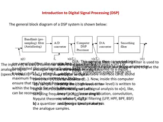
DSP processors play a crucial role in various applications such as communications, audio and video processing, graphics, navigation, radar, and more. These processors are designed to efficiently handle repetitive numerical calculations, maintain numeric fidelity, and provide real-time processing capabilities while minimizing execution unpredictability, power consumption, and development time. They feature specialized memory architecture, parallel execution units, addressing modes, instruction sets, and peripherals to meet the demands of modern signal processing tasks.

Download Presentation

Please find below an Image/Link to download the presentation.
The content on the website is provided AS IS for your information and personal use only. It may not be sold, licensed, or shared on other websites without obtaining consent from the author.If you encounter any issues during the download, it is possible that the publisher has removed the file from their server.
You are allowed to download the files provided on this website for personal or commercial use, subject to the condition that they are used lawfully. All files are the property of their respective owners.
The content on the website is provided AS IS for your information and personal use only. It may not be sold, licensed, or shared on other websites without obtaining consent from the author.
E N D
Presentation Transcript
UNIT-5 Introduction to DSP Processors By Srikanth.I Assoc.Prof, ECE Dept Methodist College of Engineering and Technology
Common DSP Applications Communications Audio, Video processing Graphics, 3-D rendering Navigation, radars, GPS Controls Robotics, guidance, Machine Vision Filtering Frequency-Time transformations (FFT-IFFT)
Common DSP Tasks Modulation-Demodulation, Error correction Noise reduction, equalization, echo cancellation Audio compression Vector and Matrix calculations Control algorithms
DSPs Need to Do Efficient repetitive numerical calculations Maintain numeric fidelity Provide high memory bandwidth Streaming data Real Time processing
DSPs Need to Minimize Real Time execution unpredictability Memory use Power consumption Cost Development time
What Do DSPs Have? Specialized memory architecture (Harvard) Specialized parallel execution units Specialized addressing modes Specialized instruction sets for parallelexecution Specialized peripherals
Multiply-Accumulate (MAC) Multiplication in single cycle Execution time ~ 200 ns Register Multiplier ALU Accumulator
Von Neumann Architecture 1. Fetch MAC instruction 2. Read value of x Processor Core 3. Read value of h 4. Multiply x, h and accumulate Address bus 5. Write result to memory Data bus 4 memory access operations Memory One multiplication (Code+Data)
Harvard Architecture 1. Data and Code in separate memory segments Processor Core 2. Multiple address and data buses AB1 DB1 3. Double memory bandwidth AB2 4. Simultaneous code and data fetch DB2 Memory A Memory B
Summary Von Neumann = Shares the same data bus and the same main memory for transfer storage of instructions and data of the programs. Von Neumann is better for desktop computers/high performance computers were cost to performance ratio is important. Harvard = Uses two separate buses for the transfer of data and instructions and two separate memories for storage of data and instructions. Harvard architecture is used primarily for small embedded computers and signal processing. Commonly used within CPUs to handle the cache.
Main differences Cell sizes used within the main memory are same in Von Neumann. However, Harvard allows for different cell sizes for data/instructions making effective use of resources. The programs in Harvard tend to be large. Modern computers make use of both Harvard and Von Neumann architecture. The main memory is used to store both instructions and data and they are both transferred over the data bus. However, the CPU s cache has Harvard architecture. There is a separate cache memory for instructions and data. There is also a separate data bus between these caches.
Von Neumann Architecture Advantages Not only data but also instructions of programs are stored within the same memory. This makes it easier to re-program the memory. Memory organisation is within the hands of the programmer. Data from memory and devices is accessed in the same way. The control unit gets data and instructions in the same way from one memory so simplifies the design and development of the control unit. Disadvantages Has only one data bus shared from the transfer of data transfers and instruction fetches; they must be scheduled because they cannot run simultaneously. Serial instruction processing does not allow for parallel execution of programs. Paralleled executions must be simulated later by the operating system (i.e. no pipelining) Higher chance of corruption or error as the instructions and data are stored and transferred in the same way so may be accidently rewritten by bugs in programs. All memory cell sizes are the same and so can t be different for instructions/data making it less efficient. Harvard Architecture Advantages There is less chance of corruption since data and instructions are transferred via different buses.
VLIW characteristics Multiple operations per instruction One instruction per cycle issued (at most) Compiler is in control Only RISC like operation support Short cycle times Easier to compile for Flexible: Can implement any FU mixture Extensible / Scalable However: tight inter FU connectivity required not binary compatible !! (new long instruction format) low code density Embedded Computer Architecture H. Corporaal and B. Mesman 2/18/2025 16
What is RISC? uses simple commands that can be divided into several instructions that achieve low-level operation within a single CLK cycle, as its name proposes Reduced Instruction Set . RISC Architecture The term RISC stands for Reduced Instruction Set Computer . It is a CPU design plan based on simple orders and acts fast. A reduced instruction set computer is a computer that only
This is small or reduced set of instructions. Here, every instruction is expected to attain very small jobs. In this machine, the instruction sets are modest and simple, which help in comprising more complex commands. Each instruction is of a similar length; these are wound together to get compound tasks done in a single operation. Most commands are completed in one machine cycle. This pipelining is a crucial technique used to speed up RISC machines. What is CISC? A complex instruction set computer is a computer where single instructions can perform numerous low-level operations like a load from memory, an arithmetic operation, and a memory store or are accomplished by multi-step processes or addressing modes in single instructions, as its name proposes Complex Instruction Set .
CISC Architecture The term CISC stands for Complex Instruction Set Computer . It is a CPU design plan based on single commands, which are skilled in executing multi-step operations. CISC computers have small programs. It has a huge number of compound instructions, which takes a long time to perform. Here, a single set of instruction is protected in several steps; each instruction set has additional than 300 separate instructions. Maximum instructions are finished in two to ten machine cycles. In CISC, instruction pipelining is not easily implemented.
RISC CISC 1. RISC stands for Reduced Instruction Set Computer. 2. RISC processors have simple instructions taking about one clock cycle. The average clock cycle per instruction (CPI) is 1.5 1. CISC stands for Complex Instruction Set Computer. 2. CSIC processor has complex instructions that take up multiple clocks for execution. The average clock cycle per instruction (CPI) is in the range of 2 and 15. 3. Performance is optimized with more focus on hardware. 4. It has a memory unit to implement complex instructions. 5. It has a microprogramming unit 3. Performance is optimized with more focus on software 4. It has no memory unit and uses separate hardware to implement instructions.. 5. It has a hard-wired unit of programming.
6. The instruction set is reduced i.e. it has only a few instructions in the instruction set. Many of these instructions are very primitive. 7. The instruction set has a variety of different instructions that can be used for complex operations. 6. The instruction set has a variety of different instructions that can be used for complex operations. 7. CISC has many different addressing modes and can thus be used to represent higher-level programming language statements more efficiently. 8. CISC already supports complex addressing modes 9. Only has a single register set 10. They are normally not pipelined or less pipelined 11. The complexity lies in the microprogram 8. Complex addressing modes are synthesized using the software. 9. Multiple register sets are present 10. RISC processors are highly pipelined 11. The complexity of RISC lies with the compiler that executes the program 12. Execution time is very less 12. Execution time is very high
13. Code expansion can be a problem 13. Code expansion is not a problem 14. The decoding of instructions is simple. 15. It does not require external memory for calculations 14. Decoding of instructions is complex 15. It requires external memory for calculations 16. The most common RISC microprocessors are Alpha, ARC, ARM, AVR, MIPS, PA-RISC, PIC, Power Architecture, and SPARC. 16. Examples of CISC processors are the System/360, VAX, PDP-11, Motorola 68000 family, AMD, and Intel x86 CPUs. 17. RISC architecture is used in high- end applications such as video processing, telecommunications and image processing. 17. CISC architecture is used in low- end applications such as security systems, home automation, etc.
Architecture of C54x 16 bits Fixed Point processor Advanced Harvard Architecture, CISC Processor Separate memory bus structures for program & data. High degree of parallelism Multiply, load/store, add/sub to/from ACC and new address generation can be done simultaneously. Powerful Instruction set & most of the operations are of single cycle Targeted for portable devices (cellular phones, MP3 players, digital cameras ) Bus structure Has several address/data buses: 1. Program Bus (PB): carries instruction codes & immediate operands from program memory to CPU. 2. Program Address Bus (PAB): provides addresses to program memory for both read/write operations. 3. Data Bus (DB): carries data between data memory space and CPU. 4. Data Address Bus (DAB): provides addresses to access data memory.
Buses in C54x 8 major 16-bit buses 4 program / data buses 1. Program bus, PB 2. Data buses 4 address buses PAB, CAB, DAB & EAB All CPU registers, peripheral registers and I/O ports occupy data memory space Memory organization Minimum address range of 192K words 64K words for program space 64K words for data space 64K words for I/O space ROM, DARAM, SARAM, two way shared RAM On-chip Memory Security option MMR: 26 CPU regs, peripheral regs and scratch pad RAM block located on data page 0(DP0) CB & DB for READ EB for Write
Central Processing Unit CPU Registers 40-bit ALU Two 40-bit Acc Regs (AccA & AccB) Barrel Shifter Supporting 0-31 bit left shift & 0-16 bit right shift range MAC Block 16-bit Temp Reg (T) 16-bit Transition Reg (TRN) Compare, Select and Store Unit (CSSU) Exponent Encoder
Accumulators A & B guard bits are helpful to prevent overflow in iterative computations like convolution/correlation
CPU registers IMR, IFR ST0 & ST1 PMST AR0 AR7(GPRs) SP reg Circular-Buffer size Register (BK) Block-Rep Regs (BRC, RSA and REA) PC Extension Reg (XPC) ST0,ST1,PMST registers
summary TMS320C5x DSP PROCESSORS FAMILY Features provided by the 54x DSPs include: 1) High-performance, low-power C54x CPU Advanced multibus architecture with three separate 16-bit data memory buses and one program memory bus 40-bit arithmetic logic unit (ALU), including a 40-bit barrel shifter and two independent 40-bit accumulators 17- 17-bit parallel multiplier coupled to a 40-bit dedicated adder for non pipelined single-cycle multiply/accumulate (MAC) operation Compare, select, and store unit (CSSU) for the add/compare selection of the Viterbi operator Exponent encoder to compute an exponent value of a 40-bit accumulator value in a single cycle Two address generators with eight auxiliary registers and two auxiliary register arithmetic units (ARAUs) Data buses with a bus holder feature Extended addressing mode for up to 8M 16-bit maximum addressable external program space Single-instruction repeat and block-repeat operations for program code
Block-memory-move instructions for better program and data management Instructions with a 32-bit-long word operand Instructions with two- or three-operand reads Arithmetic instructions with parallel store and parallel load Conditional store instructions Fast return from interrupt 2) On-chip peripherals Software-programmable wait-state generator and programmable bank- switching Phase-locked loop (PLL) clock generator with internal crystal oscillator or external clock source Full-duplex standard serial port Time-division multiplexed (TDM) serial port Buffered serial port (BSP) Multichannel buffered serial port (McBSP) Direct memory access (DMA) controller 8-bit parallel host-port interface (HPI) Enhanced 8-bit parallel host-port interface (HPI8) 16-bit parallel host-port interface (HPI16) 16-bit timer with 4-bit prescaler Interprocessor first-in first-out (FIFO) unit (on multiple CPU devices)
3) Power conservation features Software power consumption control with IDLE1, IDLE2, and IDLE3 power-down modes Ability to disable external address bus, data bus, and control bus signals under software control Ability to disable CLKOUT under software control Low-voltage device options to reduce power consumption without compromising performance 4) On-chip scan-based emulation capability IEEE 1149.1 (JTAG) boundary scan test capability 5) 5.0-V power supply devices with speeds up to 40 million instructions per second (MIPS) (25-ns instruction cycle time) 6) 3.3-V power supply devices with speeds up to 80 MIPS (12.5-ns instruction cycle time) 7) 2.5-V power supply devices with speeds up to 100 MIPS (10-ns instruction cycle time) 8) 1.8-V power supply devices with speeds up to 200 MIPS (10-ns instruction cycle time per CPU core) 9) 1.5-V power supply devices with speeds up to 532 MIPS (7.5-ns instruction cycle time per CPU core)
Addressing Modes in TMS320C54X Processor The method of specifying the operand or the data to be operated by the instruction. 1) Immediate addressing 2) Absolute addressing 3) Accumulator addressing 4) Direct addressing 5) Indirect addressing 6) Memory mapped register addressing 7) Stack addressing 1) Immediate addressing mode: The data is specified as a part of the instruction. Value encoded in the instruction. Two types of values: Short immediate (3/5/8/9- bit constant) Long immediate (16 bits) # indicates immediate. Example: LD #5, ARP ; load the immediate 3-bit constant(5h) LD #143h, DP ; load the immediate 9-bit constant(143h) in DP LD #80h, A ; 8-bit constant LD #1000h, A ; 16-bit constant
2) Absolute Addressing Mode: In this the 16-bit address of the operand is directly This addressing can be used to address an operand in all the three address spaces of the processor(i.e. address an operand in program memory, data memory and I/O ports) Complete address is specified Address is always of 16-bits 4 types: dmad addressing pmad addressing PA addressing *(lk) addressing Example: MVKD SAMPLE,*AR5 ; dmad addr MVDK *AR3, DATA1 ; dmad addr MVPD COEFF, *AR7 ; pmad addr MVPD COEFF, *AR7 ; pmad addr PORTR FIFO, *AR5 ; PA addr LD *(BUFFER), A; *(lk) addr
3) Accumulator Addressing Mode: In this the contents of accumulator is the address of the operand/data in program memory. Use Acc (A/B) contents as address. Used to address program memory as data. Two instructions: READA Smem WRITA Smem 4) Direct Addressing Mode: In this the lower 7 bits of data memory address are specified in the instruction itself. The 16-bit data memory address is formed by using either the 9 bits of DP(Data Pointer) in status register-0 or the 16-bit of SP(Stack Pointer) When DP is used, the 9 bits of DP is the upper 9 bits of the 16-bit address and the lower 7 bits are the address directly specified by the instruction. When SP is used, the 16-bit content of SP is added to 7 bits specified in the instruction to form 16-bit address. Example: ADD 6ch,A ; Add the content of memory directly addressed by the instruction to Accumulator SUB 57h,B; Subtract the content of memory directly addressed by the instruction to Accumulator B
5) Indirect addressing In this the data memory address is specified by the content of one of the eight auxiliary registers, i.e. AR0-AR7 The AR(Auxiliary Register) currently used for accessing the data is denoted by 3-bit ARP(Auxiliary Register Pointer) In this addressing mode, the content of AR can be updated automatically either after or before the operand is fetched. Example: LD *AR3,A ; load the content of memory addressed by AR3 in accumulator A LD *AR3-,A ; same as above, but after loading decrement AR3 LD *AR3+,A ; same as above, but after loading increment AR3 LD *AR3-0,A ; same as above, but after loading decrement AR3 using AR0 LD *AR3+0,A ; same as above, but after loading increment AR3 using AR0
6) Memory mapped register addressing In this the address of the memory-mapped register is specified as direct or indirect address in the instruction. Example: LDM 06h,A ; Load the content of MMR directly addressed by the instruction in accumulator A STLM A, 1Eh ; Store the content of accumulator A in MMR directly addressed by the instruction 7) Stack addressing In this the data memory address is the content of Stack Pointer(SP) The PUSH and POP instruction access the stack memory using the stack addressing mode. The CALL interrupt and RETURN instructions also use stack pointer address for automatic storage/retrieval of information to/from stack. Example: PSHM 1ch ; Decrement SP by 2 and push the content of MMR addressed by the instruction(address=1Ch) to stack memory addressed by SP POPM 1Ch ; POP the top of stack pointed by SP to MMR addressed by the instruction(address=1Ch), then SP in incremented by 2
INSTRUCTION SET OF TM320C54X PROCESSORS 1) Arithmetic instructions 2) Logical instructions 3) Branch/control instructions 4) Load/store instructions 5) Move instructions


")


 Power conservation features")

 Absolute Addressing Mode:")
 Accumulator Addressing Mode:")
 Indirect addressing")
 Memory mapped register addressing")