High-Efficiency Power Amplifier Design for 190-210GHz Range
Optimizing for high efficiency at OP1dB, this work presents a power amplifier operating in the 190-210GHz range with an output power of 17.7-18.5dBm and PAE of 6.9-8.5%. Utilizing a 250nm InP HBT process, the amplifier integrates four stages and demonstrates a gain of approximately 23dB. Key design features include low-loss compact combiners and driver scaling for sustained PAE. Accurate power measurement at the linear region is crucial for performance evaluation.
Download Presentation

Please find below an Image/Link to download the presentation.
The content on the website is provided AS IS for your information and personal use only. It may not be sold, licensed, or shared on other websites without obtaining consent from the author.If you encounter any issues during the download, it is possible that the publisher has removed the file from their server.
You are allowed to download the files provided on this website for personal or commercial use, subject to the condition that they are used lawfully. All files are the property of their respective owners.
The content on the website is provided AS IS for your information and personal use only. It may not be sold, licensed, or shared on other websites without obtaining consent from the author.
E N D
Presentation Transcript
A 190-210GHz Power Amplifier with 17.7- 18.5dBm Output Power and 6.9-8.5% PAE A. Ahmed1,2, U. Soylu2, M. Seo3, M. Urteaga4, J. Buckwalter2, and M. Rodwell2 1Marki Microwave Inc., CA 2ECE, University of California, Santa Barbara, USA 3ECE, Sungkyunkwan University, South Korea 4Teledyne Scientific Company, Thousand Oaks, CA, USA Th02C.2
Outline Motivation for mm-wave frequencies and prior work. Application for the amplifier. Amplifier design Power and driver cells Low-loss compact combiner Measurement results Summary and conclusion 2 Th02C.2
mm-wave Communication (140-1000 GHz) Objective Support high data rate communication. Spatial multiplexing for high capacity. Cover long distance. Benefits (140- 1000 GHz) Large available spectrum, high data rate. Shorter ?: more channels for the same array size. Challenge Atmospheric attenuation is high ????2 ?2? ??. 3 Th02C.2
Prior Work at G-band At 200GHz, CMOS shows 9.4dBm with only 1.03% PAE [2]. SiGe shows 13.5dBm with ~2% drain efficiency [3] GaN demonstrates higher power with <2.4% peak PAE [4], [5]. InP presented the highest power and efficiency [6]-[18]. Key points Designs are not optimized for the highest PAE at OP1dB.PAE at OP1dB<3% Power measurement accuracy at the linear region is challenging. 4 Th02C.2
This Work (190-210GHz) Optimize for the highest efficiency at OP1dB. OP1dB~17.4dBm, PAE: 6.4% at OP1dB, Gain~23dB. Accurate power measurement at the linear region. This amplifier is integrated to a 200GHz transmitter (not published). 2,900 x 1,200 (um2) PA this work 4 cells 200GHz transmitter, not published 5 Th02C.2
250nm InP HBT Process (Teledyne[6]) Mm-wave amplifier requires fast technologies. fmax=650GHz. BVCEo=4.5V. Jmax=3mA/ m. Four Au interconnect. MIM cap (0.3fF/ m2). TFR (50 /square). Cross section of TSC250 IC 6 Th02C.2
Power Amplifier Design Four stages amplifier. Combine four power cells. Driver scaling sustains good PAE. Power combining techniques Parallel combining: 4:1 transmission line combiner. Series combiner: stacked unit cell. 96- m HBT periphery 48- m HBT periphery 24- m HBT periphery 24- m HBT periphery Amplifier micrograph Amplifier block diagram 7 Th02C.2
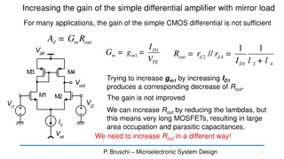
Power Cell Design CB architecture with finite base impedance. Superior PAE at OP1dB, compared to CE or grounded CB, due to the feedback linearization [14]. Base capacitances Maximum value: limited by the self resonance frequency. Minimum value: limited by the acceptable gain. Shunt transmission lines tunes the transistor parasitics. Each cell requires ~29 load impedance. Matching considerations Staggered tuning for better bandwidth. Input impedances are close to the loadline of the driver to ensure proper saturation. Transistor footprint with cap ZL~29 Power cell schematic 8 Th02C.2
Combiner Design Transmission line combiners have low loss and very compact [14], [15], [17]. Low loss 4:1 transmission line combiner. Combiner transforms 50 to the required loadline impedance for each cell (~29 ) using a single ?/4 transmission line. Each two cells are combined by a TL with negligible electrical length. The required impedance for the two combined cells is 29/2 The quarter line s impedance is chosen to transform 100 to 29/2 9 Th02C.2
Driver Cell Design Design is similar to the power cell. Architecture uses CB with finite base capacitance. Conservative driver scaling ensures hard compression characteristics at the expense of PAE degradation. Driver cell Amplifier block diagram 10 Th02C.2
Measurement Results: s-parameters Good agreement at low bias Some deviations are observed at higher bias-> maybe heating effect. 30 30 |S21| |S21| 20 20 |S21|, |S11|,|S22|, dB measured 1-dB BW>17.6GHz simulated 1-dB BW=34GHz |S21|, |S11|,|S22|, dB measured 1-dB BW=7GHz simulated 1-dB BW=32GHz 10 10 measured 3-dB BW>25.6GHz simulated 3-dB BW=50GHz measured 3-dB BW>20.5GHz simulated 3-dB BW=50GHz 0 |S22| 0 |S22| -10 -10 |S11| |S11| -20 -20 simulated measured simulated measured (a) (b) -30 -30 180 200 220 240 260 180 200 220 240 260 Freq , GHz Freq , GHz S-parameters at PDC=444mW S-parameters at PDC=858mW 11 Th02C.2
Power Measurement: literature Conventional measurement: attenuator after a frequency multiplier chain. Power sweep: change the attenuator settings. Cons The actual input power is unknown-> less accurate results. In many cases, the attenuator is manually changed -> lift the probes and turn off the PA, not convenient. Conventional power setup 12 Th02C.2
Proposed Approach: setup The VDI s output power is sampled by a coupler and monitored by the spectrum analyzer. The spectrum analyzer readings represents the power by adding the appropriate correction factor in the calibration phase. Sweep input power: control the signal generator. Harmonic Mixer Waveguide Spectrum Analyzer N9030B ~20dB Attenuation Signal Generator N5183B x8 PM4 190-210GHz 20dB coupler 23.75-26.25GHz Proposed power setup 13 Th02C.2
Calibration phase Record the power difference (dB) between the power meter and spectrum analyzer readings. This difference is the correction factor that should be added to the spectrum analyzer readings to represents the actual input power. Harmonic Mixer Waveguide Spectrum Analyzer N9030B ~20dB Attenuation Signal Generator N5183B x8 PM4 190-210GHz 20dB coupler 23.75-26.25GHz Calibration 14 Th02C.2
Measurement Phase Sweep the signal generator power. Record the spectrum analyzer readings + the appropriate correction factors. This represents the amplifier input power after calibrating the probe losses by through measurements. Report the power meter reading. The power meter readings represent the amplifier output power after calibrating probe loss. Harmonic Mixer Waveguide Spectrum Analyzer N9030B ~20dB Attenuation GGB probes Signal Generator N5183B x8 PM4 PA 190-210GHz Measurement 20dB coupler 23.75-26.25GHz 15 Th02C.2
Pros of this measurement approach Accurate gain measurement even at very low input power. Power is swept by the signal generator -> Extremely convenient since all the measurements are done without lifting the probes or turn off the PA bias. 16 Th02C.2
Power Measurement Results Many points are recorded at different frequencies. Freq, GHz OP1dB, dBm 194 202 PAE, % at OP1dB 6.4 5.3 Psat, dBm PAE, % at Psat 18.5 18.3 17.4 16.6 8.5 7.9 Discrepancy between simulations and measurement maybe due to the probe conditions. 1000 25 1000 25 Pout Pout Gain Pout, dBm, Gain, dB, PAE % Pout, dBm, Gain, dB, PAE % 20 Gain 20 950 simulated 950 simulated measured 15 measured PDC, mW 15 PAE PDC, mW 900 900 PAE 10 10 PDC 850 850 PDC 5 5 800 0 800 0 -12 -8 -4 0 4 -15 -10 -5 Pin dBm 0 5 Pin dBm Pout, Gain, and PAE vs Pin at 194GHz Pout, Gain, and PAE vs Pin at 202GHz 17 Th02C.2
Power Measurement Results More points are taken at different frequencies. Psat=17.7-18.5dBm, with PAE=6.9-8.5% over 190-210GHz OP1dB =16-17.4dBm with PAE=4.7-6.4% over 125-150GHz 25 Gain Pout dBm, PAE %, Gain (dB) 20 Pout . 15 At saturation At OP1dB 10 PAE 5 0 190 195 200 205 210 Freq (GHz) Measured Pout with the associated PAE and gain vs. frequency reported at the peak PAE. 18 Th02C.2
State-of-the-art results Ref [7] 204 18.0 [8] 190 11 [9] [10] This work 190-210 17.7-18.5 Freq, GHz Psat, dBm Gain at Psat (dB) PAE at Psat% OP1dB, dBm PAE at OP1dB% Gain at OP1dB BW3dB, GHz Size (mm2) PDC (mW) Psat/Area mW/mm2 OP1dB /Area mW/mm2 Technology 180-260 17.5-21.5 190.8-244 16.2-18.9a 16.5 19.2 13-17.5 19-22a 13.4-16.8 4.8 15.5a 3.2a 15.5a >25 0.91 1180 9.6 3 2 27a 26 0.45 970 5.1 17.5 2.1a 23.5a 18a 1.8 2620 3.3-6.1 16.1-17.16a 2.3-3.0a 23.8-35.0a 53 1.54 1270 6.9-8.5% 16-17.4 4.7-6.4 17.9-23.1 >20.5 1.14 814 69.2 28.2 50.6 62.1 77.9 39 28 31.2 33.8 48.2 130nm InP 250-nm InP HBT This work shows a record PAE at OP1dB 19 Th02C.2
Summary Demonstration of record PAE at G-band Communication transmitter requires careful attention to the performance at OP1dB Key features for highest efficiency at OP1dB Proper cell topology: Capacitively linearized common base Higher OP1dB, and PAE Driver scaling sustains good PAE Compact and low loss transmission line network 20 Th02C.2
Acknowledgement This work was supported in part by the Semiconductor Research Corporation and DARPA under the JUMP program. The authors thank Teledyne Scientific & Imaging for the IC fabrication. 21 Th02C.2
Thank You 22 Th02C.2
References [1] M. J. W. Rodwell et al., 100-340GHz Systems: Transistors and Applications, in Proc. IEEE IEDM, 2018, pp. 14.3.1-14.3.4. [2] H. Bameri and O. Momeni, "An Embedded 200 GHz Power Amplifier with 9.4 dBm Saturated Power and 19.5 dB Gain in 65 nm CMOS," in Proc. RFIC2020, 2020, pp. 191-194 [3] M. H. Eissa and D. Kissinger, "4.5 A 13.5dBm Fully Integrated 200-to-255GHz Power Amplifier with a 4-Way Power Combiner in SiGe:C BiCMOS," 2019 IEEE International Solid- State Circuits Conference - (ISSCC), San Francisco, CA, USA, 2019, pp. 82-84. [4] M. wikli ski et al., "D-Band and G-Band High-Performance GaN Power Amplifier MMICs," in IEEE Trans. Microw. Theory Techn., vol. 67, no. 12, pp. 5080-5089, Dec. 2019. [5] M. wikli ski et al., "First Demonstration of G-Band Broadband GaN Power Amplifier MMICs Operating Beyond 200 GHz," 2020 IEEE/MTT-S International Microwave Symposium (IMS), Los Angeles, CA, USA, 2020, pp. 1117-1120. [6] M. Urteaga, Z. Griffith, M. Seo, J. Hacker, M. Rodwell, InP HBT Technologies for THz Integrated Circuits , Proc. of the IEEE, vol. 105, no. 6, pp 1051-1067, June 2017. [7] A. S. H. Ahmed, A. A. Farid, M. Urteaga and M. J. W. Rodwell, "204GHz Stacked-Power Amplifiers Designed by a Novel Two-Port Technique," 2018 13th European Microwave Integrated Circuits Conference (EuMIC), Madrid, 2018, pp. 29-32. [8] Z. Griffith, M. Urteaga and P. Rowell, "A 190-GHz High-Gain, 3-dBm OP1dB Low DC-Power Amplifier in 250-nm InP HBT," in IEEE MWCL, vol. 27, pp. 1128-1130, Dec. 2017. [9] Z. Griffith, M. Urteaga and P. Rowell, "180 265 GHz, 17 24 dBm output power broadband, high-gain power amplifiers in InP HBT," 2017 IEEE MTT-S International Microwave Symposium (IMS), Honololu, HI, 2017, pp. 973-976. [10] Z. Griffith, M. Urteaga, P. Rowell, and R. Pierson, A 50 80mW SSPA from 190.8 244GHz at 0.5mW pin, in Proc. IMS2014, 2014, pp. 1 4. [11] V. Radisic, D. W. Scott, A. Cavus, and C. Monier, 220-GHz high-efficiency InP HBT power amplifiers, IEEE Trans. Microw. Theory Techn., vol. 62, no. 12, pp. 3001 3005, Dec. 2014. [12] T.B. Reed, Z. Griffith, P. Rowell, M. Field, and M. Rodwell, "A 180mW InP HBT power amplifier MMIC at 214 GHz," in 2013 IEEE Compound Semiconductor Integrated Circuit Symposium, Monterey, CA, Oct. 2013, pp.I-4. [13] M. Bao, V. Vassilev, D. Gustafsson and H. Zirath, "G-band Power Amplifiers in 130 nm InP Technology," 2020 15th European Microwave Integrated Circuits Conference (EuMIC), Utrecht, Netherlands, 2021, pp. 5-8. [14] A. S. H. Ahmed, M. Seo, A. A. Farid, M. Urteaga, J. F. Buckwalter and M. J. W. Rodwell, "A 140GHz power amplifier with 20.5dBm output power and 20.8% PAE in 250-nm InP HBT technology," 2020 IEEE/MTT-S International Microwave Symposium (IMS), Los Angeles, CA, USA, 2020, pp. 492-495. [15] A. S. H. Ahmed, M. Seo, A. A. Farid, M. Urteaga, J. F. Buckwalter and M. J. W. Rodwell, "A 200mW D-band Power Amplifier with 17.8% PAE in 250-nm InP HBT Technology," 2020 15th European Microwave Integrated Circuits Conference (EuMIC), Utrecht, Netherlands, 2021, pp. 1-4. [16] M. Seo, A. S. H. Ahmed, U. Soylu, A. A. Farid, Y. Na, and M. J. W. Rodwell, "A 200 GHz InP HBT Direct-Conversion LO-Phase-Shifted Transmitter/Receiver with 15 dBm Output Power," submitted to 2021 IEEE Radio Frequency Integrated Circuits Symposium (RFIC), Atlanta, GA. [17] A. S. H. Ahmed, U. Soylu, M. Seo, Miguel Urteaga and M. J. W. Rodwell, " A compact H-band Power Amplifier with High Output Power," submitted to 2021 IEEE/MTT-S International Microwave Symposium (IMS), Atlanta, GA. [18] A. S. H. Ahmed, A. Simsek, M. Urteaga and M. J. W. Rodwell, "8.6-13.6 mW Series-Connected Power Amplifiers Designed at 325 GHz Using 130 nm InP HBT Technology," 2018 IEEE BiCMOS and Compound Semiconductor Integrated Circuits and Technology Symposium (BCICTS), San Diego, CA, USA, 2018, pp. 164-167. 23 Th02C.2
DC Bias Lines and Power Supply Oscillations Only two independent DC supplies -> reduce the bias complexity. one supply biases all stages collectors and the second biases the stages bases. There are many feedback loops-> potential stability problems. We noticed a potential oscillation problem at low frequencies (~GHz and lower) in earlier designs. The low frequency oscillations are not adequately modeled and does not show up in simulations. In this design, we added many bypass capacitors with series resistors to avoid out of band oscillations. There is no indication for oscillations. 24 Th02C.2
Measurement accuracy The dynamic range of the power sweep is defined as follows: The minimum input power: limited by the spectrum analyzer noise level. Spectrum analyzer with reasonable noise levels shows smooth gain curves at low input power-> get accurate results to accurately report OP1dB. The maximum power: limited by the harmonic mixer saturation limit. Harmonic Mixer Harmonic Mixer Waveguide Waveguide Spectrum Analyzer N9030B ~20dB Attenuation Spectrum Analyzer N9030B ~20dB Attenuation GGB probes Signal Generator N5183B Signal Generator N5183B x8 PM4 x8 PM4 PA 190-210GHz 20dB coupler 190-210GHz 20dB coupler 23.75-26.25GHz 23.75-26.25GHz Calibration Measurement 25 Th02C.2
Measurement accuracy Probe losses are calibrated by through measurement. Old probes show non-50 impedance which degrades the output power. So, the probes may contribute to higher losses than the one measured in the through measurement. We did the measurement with an old probe pair, and we believe that the results could be improved by a newer one. 26 Th02C.2
