Comprehensive Review of BJT CE Voltage Amplifier in Electronics Lab
This lecture provides a comprehensive review of the BJT CE voltage amplifier circuit, starting with theoretical concepts and moving towards practical implementations. It covers the operation of the BJT as a switch, the addition of resistors for current control, DC design considerations, AC voltage gain amplification, and biasing the transistor in Forward Active Mode. The lecture explains how voltage gain is achieved through effective voltage division and the importance of biasing mechanisms in transistor operation.
Download Presentation

Please find below an Image/Link to download the presentation.
The content on the website is provided AS IS for your information and personal use only. It may not be sold, licensed, or shared on other websites without obtaining consent from the author.If you encounter any issues during the download, it is possible that the publisher has removed the file from their server.
You are allowed to download the files provided on this website for personal or commercial use, subject to the condition that they are used lawfully. All files are the property of their respective owners.
The content on the website is provided AS IS for your information and personal use only. It may not be sold, licensed, or shared on other websites without obtaining consent from the author.
E N D
Presentation Transcript
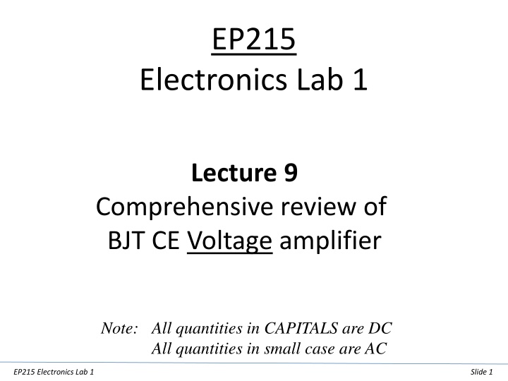
EP215 Electronics Lab 1 Lecture 9 Comprehensive review of BJT CE Voltage amplifier Note: All quantities in CAPITALS are DC All quantities in small case are AC EP215 Electronics Lab 1 Slide 1
we started with a (theoretical) BJT As a switch Vcc Ic= Ib Recall: Transistor action B Ib re E C Is this circuit PRACTICAL ? NO! Direct current path Vcc to GND EP215 Electronics Lab 1 Slide 2
98% e- from emitter are swept through the BE electric to the collector. Only ~ 2% fall into thin B : transistor
we started with a (theoretical) BJT As a switch Vcc Ic= Ib Ib re Is this circuit PRACTICAL ? NO! Direct current path Vcc to GND EP215 Electronics Lab 1 Slide 4
Add resistors to control current Our circuit immediately becomes VOLTAGE based Vcc RC vout ic= ib RB vin What is vout ? re ib What is the source of ib& vin? vout = VCC - icRC RE EP215 Electronics Lab 1 Slide 5
DC design ??? ???? ??? ????= 0 ??=??? ??? ??+ ?? EP215 Electronics Lab 1 Slide 6
AC voltage gain How (and) what is being amplified ? by transistor by the circuit large vout (~V) EP215 Electronics Lab 1 Slide 7
CE circuit amplifies a Voltage LOAD vout Ebers-M ll model C RC ???= ????= ????ie ~ ic ic = ib BJT B ????= ????= ??? vin ?? ?? ib E whatever effective resistance seen by emitter to ground RE ???? ??? = ?? ??????? ???? = ?? Where has gone? vinamplified tovoutby the (effective) voltage division of VCC by RC/RE EP215 Electronics Lab 1 Slide 8
Transistor must be biased in to Forward Active Mode Use some mechanism to set VBE > 0.7Valways (BE forward) Same mechanism must also set VCB < 0.7V always (CB reverse) Voltage gain is set by the (effective) voltage division between VCC and VE EP215 Electronics Lab 1 Slide 9
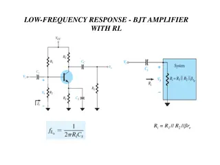
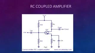
Simple resistor divider bias Vcc RC R1 vout vin re R2 RE C2 Why is C2 bad? It forces the AC gain to be RC/re EP215 Electronics Lab 1 Slide 10
To set Gain, we must add R3 Vcc RC R1 vout vin re R2 R3 RE C2 In AC, (re + R3 || RE) provides the lower leg of the voltage divider Room for improvement Have assumed infinite RL : doubtful EP215 Electronics Lab 1 Slide 11
Add immunity to load RL Vcc RC vout RB RL vin re R3 RE C2 When RL changes (decreases) : VC = VL = ILRL decreases EP215 Electronics Lab 1 Slide 12
Add immunity to load RL Vcc RC vout RL RB vin re R3 RE C2 If VC decreases, VCE also decreases (VE held fixed by DC design) So the Q point wants to shift left on IC / VCE characteristic IC Q VCE EP215 Electronics Lab 1 Slide 13
Add immunity to load RL Vcc RC However the design wants: IRc = (IC + IL) = ( IB + IL) to be fixed ( IB + IL) tends to stay fixed vout RL RB vin re R3 RE C2 IL increases with lower RL IB = (Vc VB)/RB decreases as Vc decreases So Ic = Ib wants to decrease IC Q To first order, the Q point is stabilized VCE EP215 Electronics Lab 1 Slide 14
Summary we have evolved the CE voltage amplifier Lab 5 : BJT IC v/sVCEcharacteristic in CE mode Lab 6 : Simple resistor divider with fixed gain RC / re Lab 7 : Resistor divider with gain set by R3 Lab 8+9 : Bias stabilized by collector feedback EP215 Electronics Lab 1 Slide 15
BUT Real-world devices are driven by CURRENT AC Motor: current in a coil rotor moves by induced (rotating) B field Audio speaker: current in a coil pulls magnet back and forth, cone attached to magnet vibrates sound Transistor: current in base Collector current changes proportionally EP215 Electronics Lab 1 Slide 16
Are we wasting amplified CURRENT? LOAD vout C RC ic = ib BJT B vin ib E RE LOAD ie ~ ic = ib If ie drives a load we get amplified current But beware! We must make sure that BJT bias sets it in Forward-Active ALWAYS EP215 Electronics Lab 1 Slide 17
References: Horowitz and Hill, The Art of Electronics Chapter 2 Transistors Clarify in particular, concept of small signal ac voltage gain EP215 Electronics Lab 1 Slide 18
How to calculate RB for collector feedback bias? KVL in the BE loop: -VCC + IRcRC + IBRB + VBE +IERE = 0 Simplify with IE= ( +1)IB and the usual operating conditions VC = 0.5VCC VE=0.1VCC : RE = 0.1VCC/ICQ RC = 0.5VCC/ICQ RB =[ VCC IE(RC+RE) 0.7V] / [ IE/( +1) ] with IE = ICQ EP215 Electronics Lab 1 Slide 19
