CMOS Amplifiers: Types, Analysis, & Applications

C
M
O
S
A
M
P
L
I
F
I
E
R
S
•
Introduction to Op Amp
•
Types of amplifiers
–
Simple Inverting Amplifier
–
Differential Amplifiers
–
Cascode Amplifier
–
Output Amplifiers
•
Components
–
Current mirrors
–
Current sources, current sinks
–
Voltage and current references
–
Switches, resistors, capacitors

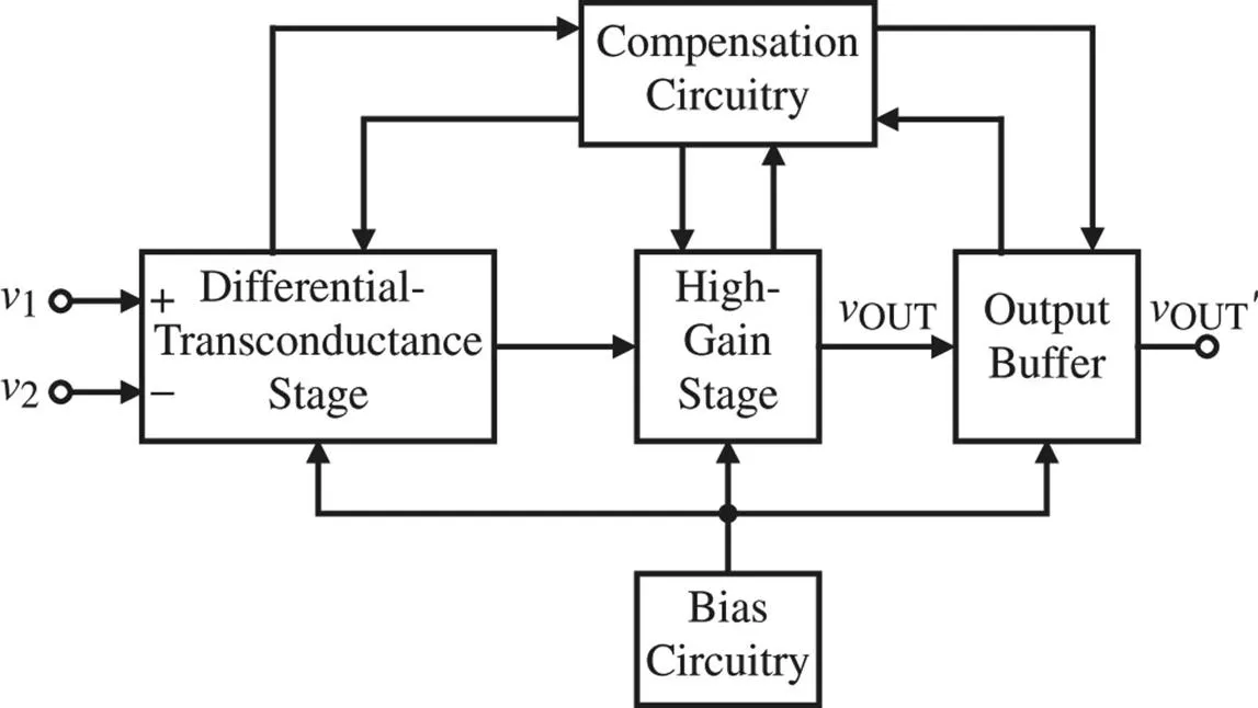
Op Amp structure
Types of Amplifiers
Common source, input pairs, are transconductance
Most whole CMOS op amps are transconductance
Common gate can be viewed as current amplifier
Current mirrors are current amplifier
Common drain or source follower is voltage amplifier
Can cascade two or more basic one to get new types
Single transistor amplifiers,
building blocks
R
in
=
R
out
=
R
in
=
R
out
=
R
in
=
R
out
=
Amplifier Notation
Analysis of amplifiers
•
DC analysis
–
Find DC operating points, i.e., quiescent point, or Q point
–
Finding the quiescent voltages V
XXQ
’s at various nodes
–
Finding I
XXQ
’s through various branches
•
Large signal static analysis
–
Plot of output versus input (transfer curve)
–
Large signal gain
–
Output and input swing limits
•
Small signal static and AC analysis
–
DC gain A0, AC gain A(s)
–
Input resistance/impedance, output resistance/impedance
•
Small signal dynamic analysis
–
Bandwidth, overshoot, settling
–
Noise
–
Power supply rejection
•
Large signal dynamic analysis
–
Slew rate
–
Nonlinearity
Simple Inverting Amplifiers
Common source with diode load
v
IN
v
OUT
V
TN
|V
TP
|
V
DD
V
GS
-V
TN
v
odP
v
odN
M1 cutoff
M2 sat
M1/2 sat
M1 tiode
M2 sat
I
D
= ½
P
(V
DD
-v
OUT
-|V
TP
|)
2
(1+
P
V
DD
-v
OUT
)) = ½
N
(v
IN
-V
TN
)
2
(1+
N
v
OUT
)
V
DD
Large signal limits
Absolute limits: None for v_in
v_out: v_out at Vin=V
DD
to V
DD
-V
TP
To have all transistors in saturation:
Vin range:
Vout range:
Small Signal Characteristics
Inverter with diode connection load
High gain inverters
Current source load or push-pull
•
Refer to book for large signal analysis
•
Must match quiescent currents in PMOS
and NMOS transistors
•
Wider output swing, especially push-pull
•
Much higher gain (at DC), but much lower
-3dB frequency (vs diode load)
•
About the same GB
•
Very power dependent
Small signal
High gain! Especially at low power.
Dependence of Gain upon Bias Current
Vo
Vg
Vo+
Vg
I
D
I
D
1.
Use sufficient g
m
/I
d
2.
Use sufficient L
3.
Use sufficient V
ds-Ex
B
u
t
:
L
a
r
g
e
r
L
r
e
d
u
c
e
s
f
T
,
s
l
o
w
s
d
o
w
n
o
p
e
r
a
t
i
o
n
.
V
D
S
f
r
e
e
d
o
m
i
s
l
i
m
i
t
e
d
:
i
n
t
h
e
2
n
d
s
t
a
g
e
V
D
S
r
a
n
g
e
i
s
l
a
r
g
e
r
b
u
t
m
u
s
t
m
e
e
t
V
o
s
w
i
n
g
r
e
q
u
i
r
e
m
e
n
t
;
1
s
t
s
t
a
g
e
V
D
S
r
a
n
g
e
i
s
q
u
i
t
e
s
m
a
l
l
.
S
m
a
l
l
c
u
r
r
e
n
t
d
e
n
s
i
t
y
a
l
s
o
l
e
a
d
s
t
o
s
l
o
w
o
p
e
r
a
t
i
o
n
.
3
w
a
y
s
t
o
i
n
c
r
e
a
s
e
A
0
:
l
a
r
g
e
r
L
,
s
u
f
f
i
c
i
e
n
t
V
D
S
,
a
n
d
s
m
a
l
l
c
u
r
r
e
n
t
d
e
n
s
i
t
y
.
Key to analysis by hand:
•
Use level 1 or 3 model equations
•
Use KCL/KVL
Transfer function of a system
System
input u
output y
poles
zeros
For stability
•
All closed loop poles must have negative
real parts
–
But open loop poles do not need to be stable
–
Feedback changes the location of the poles
•
Location of zeros cannot be changed by
feedback
–
Right half plane zeros do not cause instability
by themselves
–
But they have very negative impact on phase
margin, making stabilization more difficult
Nodal analysis
•
Identify nontrivial nodes
•
Write a KCL at each node
•
Solve for TF from input to output
Frequency Response of CMOS Inverters
Only one non trivial node
KCL:
Y
tot
V
out
(s)=I
inj
Y
tot
=gds1+gds2+sCgd1
+sCBD1+sCL+sCBD2
+sCGD2
=go+sCL’
I
inj
=-gm1vin+sCGD1vin
CMOS Inverters
Let x=vin
Still only one non trivial node
KCL:
Y
tot
V
out
(s)=I
inj
Same Y
tot
=gds1+gds2+sCgd1
+sCBD1+sCL+sCBD2
+sCGD2
=go+sCL’
But I
inj
=-gm1vin+sCGD1vin –gm2vin+sCGD2vin
Input output transfer function
When s=j
0, A(0)
When w
∞, A(s)
BW:
|p
1
|=
g0/CL’
|z
1
|
=gm/Cgd
=GB*CL’/Cgd
|A
0
| =gm/go
0 dB
gain BW
product
=|A
0
p
1
|
=GB
=gm/CL’
A
cl
=1/
Unity gain
frequency of
Loop gain A
=-3dB frequency
of closed loop
=
*GB
gain
Unity gain feedback
A(s)
Closed-loop zero: z
1
F
e
e
d
b
a
c
k
c
h
a
n
g
e
d
p
o
l
e
l
o
c
a
t
i
o
n
,
b
u
t
d
o
e
s
n
o
t
c
h
a
n
g
e
z
e
r
o
l
o
c
a
t
i
o
n
.
If a step input is given, the output response is
By the final value theorem:
By the initial value theorem:
Final settling determined by A
0
need high gain
Settling speed determined by A
0
p
1
=GB=UGF,
need high gain bandwidth product
-1
R
i
g
h
t
h
a
l
f
p
l
a
n
e
z
e
r
o
c
a
u
s
e
s
i
n
i
t
i
a
l
r
e
v
e
r
s
e
t
r
a
n
s
i
e
n
t
,
w
h
o
s
e
s
i
z
e
d
e
p
e
n
d
s
o
n
m
a
i
n
p
o
l
e
/
z
e
r
o
r
a
t
i
o
.
Gain bandwidth product
C’
L
= C
total
= C
GD1
+ C
GD2
+ C
BD1
+ C
BD2
+ C
L
If fixed V
EB
used, W, I
D
, g
m
increase in proportion;
GB initially increases but saturates near C’
L
=2C
L
.
Gain bandwidth product: I
D
bias
For small C
L
W
1
GB
0
At max GB sizing
•
Use large current density
•
Use small L
•
Use NMOS for larger
•
Use smallest drain area
•
Use larger V
D
•
Large Cox: thin oxide and high K
•
Small gate drain overlap
L, small side wall
capacitance density
Max GB and slew rate
Note:
If V
EB1
and V
EB2
are fixed, W1/L1 and W2/L2
must be adjusted proportionally, and they are
proportional to DC power.
Therefore:
P is proportional to W1, W2
C
L
constant, but C(W
1
,W
2
) proportional to W1, W2
When C(W1, W2) << CL, GB proportional to P
When C(W1,W2)
CL or >CL, GB saturates
P
GB
Linear increase region
N
O
I
S
E
I
N
M
O
S
I
N
V
E
R
T
E
R
S
To minimize:
1)
L2 >>L1
2)
e
n1
small
For thermal noise
Delve into the world of CMOS amplifiers with an exploration of different types such as inverting, cascode, and differential amplifiers. Understand the components, including current mirrors and sources, along with voltage and current references. Dive into the analysis of amplifiers, from DC and AC characteristics to large signal dynamics. Explore common building blocks like single transistor amplifiers and unravel the complexities of amplifier notation. Discover the intricacies of amplifier circuits, their operation, and practical applications.

Download Presentation

Please find below an Image/Link to download the presentation.
The content on the website is provided AS IS for your information and personal use only. It may not be sold, licensed, or shared on other websites without obtaining consent from the author.If you encounter any issues during the download, it is possible that the publisher has removed the file from their server.
You are allowed to download the files provided on this website for personal or commercial use, subject to the condition that they are used lawfully. All files are the property of their respective owners.
The content on the website is provided AS IS for your information and personal use only. It may not be sold, licensed, or shared on other websites without obtaining consent from the author.
E N D
Presentation Transcript
CMOS AMPLIFIERS Introduction to Op Amp Types of amplifiers Simple Inverting Amplifier Differential Amplifiers Cascode Amplifier Output Amplifiers Components Current mirrors Current sources, current sinks Voltage and current references Switches, resistors, capacitors
Types of Amplifiers Common source, input pairs, are transconductance Most whole CMOS op amps are transconductance Common gate can be viewed as current amplifier Current mirrors are current amplifier Common drain or source follower is voltage amplifier Can cascade two or more basic one to get new types
Single transistor amplifiers, building blocks Rin = Rout = Rin = Rout = Rin = Rout =
Analysis of amplifiers DC analysis Find DC operating points, i.e., quiescent point, or Q point Finding the quiescent voltages VXXQ s at various nodes Finding IXXQ s through various branches Large signal static analysis Plot of output versus input (transfer curve) Large signal gain Output and input swing limits Small signal static and AC analysis DC gain A0, AC gain A(s) Input resistance/impedance, output resistance/impedance Small signal dynamic analysis Bandwidth, overshoot, settling Noise Power supply rejection Large signal dynamic analysis Slew rate Nonlinearity
Common source with diode load vOUT VDD |VTP| M1/2 sat vodP M1 cutoff M2 sat vodN M1 tiode M2 sat vIN VDD VTN ID = P(VDD-vOUT -|VTP|)2(1+ P(VDD-vOUT)) = N(vIN-VTN)2(1+ NvOUT)
Large signal limits Absolute limits: None for v_in v_out: v_out at Vin=VDD to VDD-VTP To have all transistors in saturation: Vin range: Vout range:
Inverter with diode connection load Small Signal Characteristics = = v g g 1 1 out v m m A v + + g g g g 1 2 2 2 in ds ds m m ' N v V V K K W L W L W L W L = = = A out v odP N 1 2 1 2 v ' 2 1 2 1 in odN P P 1 1 = out r + + g g g g 1 2 2 2 ds ds m m
Current source load or push-pull Refer to book for large signal analysis Must match quiescent currents in PMOS and NMOS transistors Wider output swing, especially push-pull Much higher gain (at DC), but much lower -3dB frequency (vs diode load) About the same GB Very power dependent
Small signal + + v g g g g 1 2 v g = = = = 1 2 out v m m A A 1 g out v m A A 0 v 0 v + g 1 2 in ds ds 1 2 in ds ds g g = Transistor intrinsic voltage gain: m A 0 ds g I = 2 g I ds D m D 2 I K I = = D A 0 I D D High gain! Especially at low power.
Dependence of Gain upon Bias Current ID ID + Vg Vo+ + Vg Vo
2 C 2 ox 2 I K I L 2 = = = = D A 0 I I I W D D D D K qN 0 s K K = 0 s A 0 ox t C 2 + + ox 2 ( ) 2 ( ) L f V L qN V 2 2 D ch D ch 0 0 A ox K qN L V + 4 ( t K I ) DSAT V 0 ox A DS ox s A 0 D W
1 g g g I = = A m m 0 ds D K 0 s 2 + 2 ( ) L qN V 2 D ch 0 A 1. Use sufficient gm/Id 2. Use sufficient L 3. Use sufficient Vds-Ex
3 ways to increase A0: larger L, sufficient VDS, and small current density. But: Larger L reduces fT, slows down operation. VDS freedom is limited: in the 2nd stage VDS range is larger but must meet Vo swing requirement; 1st stage VDS range is quite small. Small current density also leads to slow operation.
Key to analysis by hand: Use level 1 or 3 model equations Use KCL/KVL C W = + ( ) (1 ) 1 I v V v N ox L 2 1 D GS T N DS 2 C W L C W L C W L 1 V = + + + ( ) (1 ( )) 1 N ox V v V v 2 DD GS in T N o 2 2 1 = = + ( | |) (1 ) 2 P ox I v V V 2 2 D SG TP P DS 2 2 V = + ( | |) (1 ( )) 2 P ox V V v V v 2 DD DD GP in TP P o 2 2 2
C W C W = = = Let ,suppose | | , , 1 2 N ox L P ox L E V V TP T P N 2 2 1 2 and a battery offset ( GS DD V V C W g L C W g = is used, then operating point is: ( )/ 2, GP DD C V V E = + C = = )/ 2, / 2 E V V C o DD = (( )/ 2 ) 1 N ox V E V 1 m DD C T 1 (( )/ 2 ) 1 N ox L V E V 2 1 ds DD C T N 2 C W L C W L 1 = = (( )/ 2 ) 2 P ox g V E V g 2 1 m DD C T m 2 = (( )/ 2 ) 2 P ox g V E V 2 2 ds DD C T P 2 2
Transfer function of a system input u output y System + + + ) 1 + 1 m m ( a A b s n b s n b s = = 0 1 1 ( ) ( ) ( ) ( ) m m y s H s u s u s + + + ) 1 + 1 ( s a s a s 1 1 n n s s 1 ( 0 A ) 1 ( ) zeros z z = 1 ( ) m u s s s s 1 ( )( 1 ) 1 ( ) p p p 1 2 n poles
For stability All closed loop poles must have negative real parts But open loop poles do not need to be stable Feedback changes the location of the poles Location of zeros cannot be changed by feedback Right half plane zeros do not cause instability by themselves But they have very negative impact on phase margin, making stabilization more difficult
Nodal analysis Identify nontrivial nodes Write a KCL at each node Solve for TF from input to output KCL Y kk node at V k k : = ( ) ( ) ( ) ( ) ( ) s s Y s V s I s , kj j k inj j k ( admitance total : ) attached node to k Y s kk ( admitance : ) between node k and node j Y s kj ( injected : ) s current into node k I , k inj
Frequency Response of CMOS Inverters Only one non trivial node KCL: YtotVout(s)=Iinj Ytot =gds1+gds2+sCgd1 +sCBD1+sCL+sCBD2 +sCGD2 =go+sCL Iinj=-gm1vin+sCGD1vin
Solving for sC ( / ) g ( , ) s we get V s V o in = 1 1 ( ) GD m T s + ' g sC o L g = pole at : o p ' C L g = + 1 zero at : right , half plane m z C 1 GD
CMOS Inverters Let x=vin Still only one non trivial node KCL: YtotVout(s)=Iinj Same Ytot =gds1+gds2+sCgd1 +sCBD1+sCL+sCBD2 +sCGD2 =go+sCL But Iinj=-gm1vin+sCGD1vin gm2vin+sCGD2vin
Solving for C s ( + / ) C ( , ) s we g get + V s V o in ( ) ( ) g = 1 2 + 1 2 ( ) GD GD g m m T s ' sC o L g = pole at : , same o p ' C L + g g = + 1 2 zero at : right , half plane m m z + C C 1 2 GD GD
Input output transfer function + g g s + 1 ( ) 1 2 m m g g s + g g 1 ( 0 A ) 1 2 m m 1 2 ds ds + C C z = = 1 2 ( ) GD GD 1 A s s s + + 1 ( ) 1 ( ) g g p 1 2 ds ds 1 ' C L + g g = When s=j 0, A(0) 1 2 m m A 0 + g g 1 2 ds ds + C C C When w , A(s) 1 2 1 GD GD ' L
Unity gain frequency of Loop gain A =-3dB frequency of closed loop = *GB gain |A0 | =gm/go Acl=1/ 0 dB BW: |p1|= g0/CL gain BW product =|A0p1| =GB =gm/CL |z1| =gm/Cgd =GB*CL /Cgd
Unity gain feedback A(s) (1 A ) ( ) A s A s z A s = = 0 1 A c 1 ( ) 1 (1 ) A s z (1 (1 z p = s p ) A p A z 0 1 s z A 1 = For Closed-loop pole: 1 0 ) s p 0 1 1 ) ( + = 0 z p z 1 1 0 (1 0 ) 1 1 1 1 0 Closed-loop zero: z1 Feedback changed pole location, but does not change zero location. s A p 0 A p 0 1 1
If a step input is given, the output response is (1 ) 1 A s z = 0 1 ( ) s Y step 1 (1 ) A s z s p s 0 1 1 By the final value theorem: A = = = ( ) lim s ( ) s 0 A step y t sY step 1 0 0 By the initial value theorem: / A z z A p A p = = = = ( 0 ) + lim s ( ) s 0 1 0 1 0 z 1 y t sY step step / 1 A p z A p 0 1 1 1 0 1 1
Right half plane zero causes initial reverse transient, whose size depends on main pole/zero ratio. A p 0 z 1 1 e A p t 0 1 decay A 0 A 1 0 -1 Final settling determined by A0 need high gain Settling speed determined by A0p1=GB=UGF, need high gain bandwidth product
Gain bandwidth product + + + g g g g g g = = = 1 2 1 2 1 2 m m ds ds m m GB A p 0 1 + ' ' g g C C 1 2 ds ds L L C L = Ctotal = CGD1+ CGD2+ CBD1+ CBD2+ CL = 1 + + + + ' C C W L C W L C W L C W L C 2 1 1 2 2 L ox ox j D j D L C W C W + = + 1 2 N ox P ox g g V V 1 2 1 2 m m EB EB L L 1 2 If fixed VEB used, W, ID, gm increase in proportion; GB initially increases but saturates near C L=2CL.
Gain bandwidth product: ID bias g C = = 1 m GB A p 0 0 1 ' L 2 C W L = + + = C C CW C W 1 ox g I ' 1 1 2 2 L L 1 m D 1 2 + / C W CW L g C = = 1 ox GB I 1 m 0 D + C C W ' 1 1 2 2 L L 2 C For large : C GB W I ox 0 L D LC 2 L
For small CL GB0 W1 = + Max reached when CW C C W 1 1 2 2 L C = GB I ox + ( ) 0max D 2 LC C C W 1 2 2 L
At max GB sizing = + Max reached when CW C C W 1 1 2 2 L C C LC I W = = GB I o + x ox D ( ) 0max D 2 2 LC C C W 2 1 1 2 2 1 L Use large current density Use small L Use NMOS for larger Use smallest drain area Use larger VD Large Cox: thin oxide and high K Small gate drain overlap L, small side wall capacitance density
Max GB and slew rate 1 dv dt I C = = max max SR i o D C C tot tot L C = GB I ox + ( ) 0max D 2 LC C C W 1 2 2 L + C C W I C = ox D ( ) 2 1 / LC C 1 2 2 L L C LC I C ox D 2 1 L
NOISE IN MOS INVERTERS 2 g = + 2 out 2 n 2 n 1 m e e e 1 2 g = 0 V in 2 m 2 2 out A e g = = + 2 eq 2 n 2 n 2 m e e e 1 2 2 v g 1 m 2 2 n g e = + 2 eq 2 n 2 2 1 m e e 1 g 2 n e 1 m 1
B = = 2 For 1/f noise : ; constant en B fWL ' 2 K W = g I m D L + 1 ' 2 / K W I L B fW L = 2 2 2 2 1 1 P ' D P e e 1 eq n 2 / K W I L fW L B 1 1 2 2 N D N 2 B L L K B K B ' = + 1 N e 1 P P 2 eq W L f ' 1 1 2 N N To minimize: ' N K W L 1) L2 >>L1 2) en1 small = 1 2 gain ' K W P L 2 1
B = For 1/f noise: if holds, but square law does not: e 2 n fWL 2 g g B W L B W L B = + 1 2 m 1 1 1 2 e 2 eq W L f 1 1 1 2 2 1 m 2 g 2 m B I W L B W L B = + 1 1 1 1 2 D g W L f 1 m 1 1 2 2 1 I D So, place M1 in weak inversion and user larger L2 (and larger W2) than L1 M2 in strong inversion
But the best one can do is to make second term=0 = + 2 g 2 m B I W L B W L B B 1 e 1 1 1 2 1 D 2 eq g W L f W L f 1 m 1 1 2 2 1 1 1 I D Since B is about 6 to 10 times B , to have small , e 2 eq N P we need M1 to be PMOS and M2 t o be NMOS.
The previous slide and what is in the book works only for the case when square law works and 8 1 , 3 8 8 1 3 3 m g g = . In general: g g m do 8 kT kT ( ) ( ) = + = + 1 2 dn i g 2 dn i g 1 1 1 2 2 2 do do 3 g g kT kT ( ) ( ) = + = + 1 1 e g do 21 n 1 1 1 do 21 m 1 1 m 8 3 8 3 g g g g kT g kT g ( ) ( ) = + = + 1 1 2 2 do m e g 22 n 2 2 2 do 21 m 1 2 1 m m m Strategies: make sure gdo/gm small (close to 1) make gm1 large make gm1 /gm2 large make small ( VBS=0) and gds small