Operational Amplifiers (Op-Amps) and Their Applications
Operational Amplifiers (Op-Amps) are devices used to amplify signals using an external power source. They are composed of transistors, resistors, and capacitors. Op-Amps find applications in summing amplifiers, AC and DC signal processing, digital-to-analog converters, active filters, oscillators, regulators, rectifiers, comparators, integrators, and differentiators. The ideal Op-Amp has specific characteristics like infinite open-loop gain and infinite input impedance. Understanding Op-Amps and their various modes of operation is essential in electronics.

Download Presentation

Please find below an Image/Link to download the presentation.
The content on the website is provided AS IS for your information and personal use only. It may not be sold, licensed, or shared on other websites without obtaining consent from the author.If you encounter any issues during the download, it is possible that the publisher has removed the file from their server.
You are allowed to download the files provided on this website for personal or commercial use, subject to the condition that they are used lawfully. All files are the property of their respective owners.
The content on the website is provided AS IS for your information and personal use only. It may not be sold, licensed, or shared on other websites without obtaining consent from the author.
E N D
Presentation Transcript
US05CPHY05 UNIT - IV Operational Amplifier [OpAmp] 1
US05CPHY05 UNIT - IV Operational Amplifier [OpAmp] Reference Book: Integrated Circuits K R Botkar 2
What is an Op-Amp? An Operational Amplifier (known as an Op-Amp ) is a device that is used to amplify a signal using an external power source. Op-Amps are generally composed of: Transistors, Resistors, Capacitors = + +
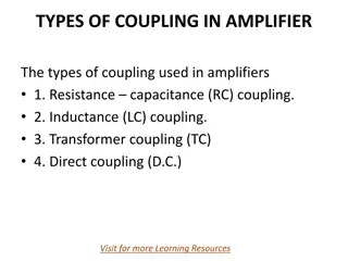
Applications of Op Applications of Op- -amp amp Summing Amplifiers AC and DC signals application Digital-to-Analog converters Analog computers Active filters [Low-Pass and High-Pass Band-Pass Filters] Oscillators Regulators Rectifiers Comparators Integrators and Differentiators etc.
Typical IC packages IC packages placed on circuit board Amplifier with ICs: Reliable Reduced Cost Reduced Size High Noise Reduction Capacity 5
Introduction- Operational Amplifier (Op-Amp) It is an integrated circuit that uses external voltage to amplify the input through a very high gain. Op-amps are used to model the basic mathematical operations; subtraction, integration and differentiation in electronic analog computers. addition, 6
Ideal Operational Amplifier Ideal Operational Amplifier Ideal op-amp is characterized by: ohms; 1. Infinite open loop gain; A = 2. Zero output R 0 o = 3. Infinite input ohms; R i 4. Zero output voltage when input is voltage is zero. 5. Infinite CMRR.
2 7 6 4 3
Op-Amp Input Modes Single-Ended Input Mode Input signal is connected to ONE input and the other input is grounded. Non- Inverting Mode input signal at +ve terminal output same polarity as the applied input signal Inverting Mode input signal at ve terminal output opposite in phase to the applied input signal 10
Op-Amp Input Modes Differential Input Mode TWO out-of-phase signals are applied with the difference of the two amplified is produced at the output. = V A V out d d = V V V 1 2 d in in 11
Op-Amp Input Modes Common Mode Input Two signals of same phase, frequency, and amplitude are applied to the inputs which results in no output (signals cancel). But, in practical, a small output signal will result. This is called common-mode rejection. This type of mode is used for removal of unwanted noise signals. 12
+Vcc Input 1 + Vo Vd Output Input 2 -Vcc Rout~0 Rin~inf
Ideal Op-Amp Infinite Voltage Gain Infinite Input Impedance Zero Output Impedance Voltage Controlled Voltage source (VCVS)
Ideal Vs Practical Op-Amp Ideal Practical 105 Open Loop gain A Bandwidth BW 10-100Hz >1M Input Impedance Zin Output Impedance Zout Output Voltage Vout 0 10-100 Depends only on Vd Differential mode signal Depends slightly on average input Vc = (V++V )/2 Common- Mode signal 10-100dB CMRR 16
Ideal Op-Amp Infinite Input Impedance Input impedance is measured across the input terminals. Input impedance is the ratio of input voltage to input current. i i I V Z = i When Zi is infinite, the input current is zero. The op amp will neither supply current to a circuit nor will it accept current from any external circuit. In real op-amp, the impedance is 500 k to 2M
Ideal Op-Amp Zero Output Impedance Looking back into the output terminal, we see it as a voltage source with an internal resistance. The internal resistance of the op-amp is the output impedance of op-amp. This internal resistance is in series with the load, reducing the output voltage available to the load Real op-amps have output impedance in the range of 20-100 . 18
Ideal Op-Amp = V A V out v in Infinite Open-Loop Gain Open-Loop Gain, A is the gain of the op-amp without feedback. In the ideal op-amp, A is infinite In real op-amp, A is 20k to 200k 19
Ideal Op-Amp Infinite Bandwidth The ideal op-amp will amplify all signals from DC to the highest AC frequencies In real op-amps, the bandwidth is rather limited This limitation is specified by the Gain-Bandwidth product, which is equal to the frequency where the amplifier gain becomes unity Some op-amps, such as 741 family, have very limited bandwidth, up to a few kHz only 20
Ideal Op-Amp Zero Noise Contribution In an ideal op amp, all noise voltages produced are external to the op amp. Thus any noise in the output signal must have been in the input signal as well. The ideal op amp contributes nothing extra to the output noise. In real op-amp, there is noise due to the internal circuitry of the op-amp that contributes to the output noise 21
Ideal Op-Amp Zero Output Offset The output offset voltage of any amplifier is the output voltage that exists when it should be zero. The voltage amplifier sees zero input voltage when both inputs are grounded. This connection should produce a zero output voltage. If the output is not zero then there is said to be an output voltage present. In the ideal op amp this offset voltage is zero volts, but in practical op amps the output offset voltage is nonzero (a few miliVolts). 22
Ideal Op-Amp Both Differential Inputs Stick Together this means that a voltage applied to one inverting inputs also appears at the other non- inverting inputs. If we apply a voltage to the inverting input and then connect a voltmeter between the non-inverting input and the power supply common, then the voltmeter will read the same potential on non-inverting as on the inverting input. 23
7.1 Basic Differential Amplifier Analysis 7.1.1 DC Analysis of the Bipolar Differential Amplifier Circuit
DC ANALYSIS DC bias of differential amplifier circuit + + = ( ) 0 V I R V BE E E EE V V EE BE = I E R E I E = = I I since V 0 C C B 1 2 2 I = = = E V V V I R V R 1 2 C C CC C C CC C 2
Example : Differential Amplifier Circuits Calculate the dc voltages and currents 27
Operation Example Differential Amplifier Circuit Solution V V = EE BE I E R E 7 . 0 9 V V = = 5 . 2 IE mA 3 . 3 k I 5 . 2 m = = = E . 1 25 I I mA 1 2 C C 2 2 = V V I R C CC C C = . 1 ( = 9 25 9 . 3 )( ) 1 . 4 VC V m k V 28
Four Possible Configurations Dual Input, Balanced Output Configuration Dual Input, Un-balanced Output Configuration Single Input, Balanced Output Configuration Single Input, Un-balanced Output Configuration
Differential Amplifier Circuit AC ANALYSIS Single-Ended Connection to calculate : Av1 = Vo1 / Vi1 30
Differential Amplifier Circuit Single-Ended AC ANALYSIS C B E AC equivalent of differential amplifier circuit 31
Differential Amplifier Circuit AC Analysis - Single ended KVL = + V I r I r i b i b i 1 I V = = T Note : r r V 2 i i r = I CQ 1 b Scan figure 10.11 & 10.15 r = i i Hence r e V i = = I I 1 c b 2 r i V R R i c = = = c V I R V Partial circuit for calculating Ib 1 r o c c i 2 2 r 1 i e = = V R 2 1 2 = = o c A = = I I I v = = V r r r r b b b i e 1 2 i i i 1 32 1 2
Differential Amplifier Circuit Example Solution 7 . 0 7 . 0 9 V V V V = = = 193 EE I A E 43 R k E = = 75 1 2 I = = E 96 5 . I A C 2 V = V I R c cc c c = = 9 96 ( 5 . )( 47 ) 5 . 4 Vc k V V 26 = = = T 269 r e = = 9 96 ( 5 . )( 47 ) 5 . 4 V A k V 0965 . 0 I CQ Calculate the single-ended output voltage Vo1 = T V 47 R k = = = 87 4 . c A v 2 ( 2 269 ) r = 26 mV e = = 87 ( 4 . )( 2 ) . 0 175 V A V m V = = 20 r r k 1 o v i i i 33 1 2
Differential Amplifier Circuit AC Analysis - Double ended A similar analysis can be used to show that for the condition of signals applied to both inputs, the differential voltage gain magnitude is V R = = o c A d 2 V r d i = where V V V 1 2 d i i 34
Differential Amplifier Circuit AC Analysis - Common-mode Common-mode connection 35
Differential Amplifier Circuit AC Analysis - Common-mode ) 1 + ( 2 V I R = i b E I V R + b r i c = = = V I R I R 1 i o c c b c + ( 2 ) 1 r R Rearrangin g, i E V R V = = o c + A = i I v + ( 2 ) 1 V r R b + ) 1 + ( 2 r R 36 i i E i E
Distortion +Vcc=+5V +5V + Vo Vd 0 5V Vcc= 5V The output voltage never excess the DC voltage supply of the Op-Amp 37
Common-Mode Operation + Same voltage source is applied at both terminals Vo Ideally, two input are equally amplified Vi ~ Output voltage is ideally zero due to differential voltage is zero Note for differential circuits: Opposite inputs : highly amplified Common inputs : slightly amplified Practically, a small output signal can still be measured. Common-Mode Rejection Operational Amplifier 38
Common-Mode Rejection Ratio (CMRR) Differential voltage input : + = V Vd Noninverting Input + V Output Inverting Input Common voltage input : 1 = V Vc ++ ( ) V 2 Common-mode rejection ratio: G G = = d d CMRR 20 log ( dB ) Output voltage : = 10 G G c c + V G V G V o d d c c Note: When Gd >> Gc or CMRR Vo = GdVd Gd : Differential gain Gc : Common mode gain 39
CMRR Example What is the CMRR? 100V 100V + + 60700V 80600V 40V 20V Solution : = = = = V V 100 20 80 100 40 60 V V 1 2 d d (2) (1) + + 100 20 100 40 = = = = V V 60 70 V V 1 2 c c 2 2 = + = From (1) V 80 60 80600 V G G o d c = + = From G (2) 1000 V 60 G 70 60700 V G G o d c = = = = and CMRR dB 10 20 log( 1000 / 10 ) 40 d c NB: This method is Not work! Why? 40
Applications of Op-Amp To provide voltage amplitude changes (amplitude and polarity) Comparators Oscillators Filters Sensors Instrumentation amplifiers 41


")