Understanding Picoblaze_GCD Implementation and Synthesis
Explore the implementation, simulation, and synthesis process of Picoblaze_GCD. Dive into files and instances for synthesis, FSM programming in assembly, flags manipulation, and interfacing with Picoblaze processor through input and output instructions.

Download Presentation

Please find below an Image/Link to download the presentation.
The content on the website is provided AS IS for your information and personal use only. It may not be sold, licensed, or shared on other websites without obtaining consent from the author. Download presentation by click this link. If you encounter any issues during the download, it is possible that the publisher has removed the file from their server.
E N D
Presentation Transcript
Picoblaze_GCD GCD on Picoblaze Implementation, Simulation, and Synthesis
Files and Instances for synthesis gcd_picoblaze.xdc FPGA Artix 7 ee354_GCD_picoblaze_top.v module ee354_GCD_top Output ports related fabric logic and Standard two instances of the picoblaze processor Input ports related fabric logic standard SSD scanning logic Instance name processor Instance name program_rom address[11:0] picoblaze processor kcpsm6.v Program memory BRAM prom_gcd.v produced from prom_gcd.psm instruction[17:0] module kcpsm6 module prom_gcd
FSM in Assembly We need to program each state separately in assembly Start, Step and Ack are the external Control signals used here to exercise sequencing control.
FSM in Assembly Each if/else represents a jump (conditional/unconditional)
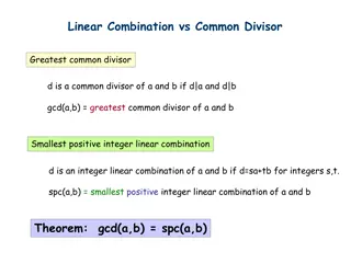
The Carry (C) and the Zero (Z) flags It is important to understand how the Arithmetic, Logical, Test, and Compare instructions change the Carry (C) and the Zero (Z) flags and further how the conditional jumps, conditional calls, and conditional returns utilize the Carry (C) and the Zero (Z) flags.
Carry, Borrow, and Odd Parity Even though the name of the flag is Carry , its meaning changes depending on the context. Logical operations (AND, OR, and XOR) will reset the carry to zero. The ADD operation will set the carry if the out-going carry C8 is true (otherwise will reset it). The COMPARE operation performs comparison by performing subtraction. The COMPARE and SUBtract operations will set the carry if the subtrahend is bigger (otherwise will reset the carry). So the carry flag can be viewed as representing the out-going borrow in subtraction. In the case of TEST instructions, AND operation is performed to see if the result is zero or if the result has odd number of 1 s as indicated by the carry flag. So the carry flag can be viewed as an Odd Parity of the result 8 bits in the case of the TEST (and an Odd Parity of the result 8 bits plus one incoming carry bit in the case of the TESTCY).
Top design - fabric logic to interface with the PicoBlaze Processor How is our top design interfacing with the picoblaze processor through the INPUT and OUTPUT instructions? Let s consider the INPUT instruction. INPUT sX, pp pp is the 8-bit port address in hex that the processor will output on port_id sX is one of the 16 8-bit registers (s0 through sf) inside the processor that will store the data coming through in_port[7:0]
In this lab, the processor informs the fabric logic in which state it is currently at (Init, Sub, Mult, Done) using the OUTPUTK instruction. Possible to do so in two ways: using OUTPUT sX, pp or using OUPUTK kk, p Suppose constant 02 (kk = 02) needs to conveyed to the output port 01 (pp = 01) LOAD s5, 02 ; OUTPUT s5, 01 OUTPUTK 02, 01 ; extract from our .psm file state_initial: OUTPUTK 00000001'b, Current_State ; Indicating Current State as Initial State
out_port interface We have two output instructions available to us, OUTPUT and OUTPUTK The regular OUTPUT instruction lets us output the 8-bit data of a register: OUTPUT sX, pp sX is the register containing the data we are outputting, pp is the 8-bit address we output on port_id, write_strobe signal goes active. The OUTPUTK instruction lets us output an 8-bit constant: OUTPUTK kk, p kk is the 8-bit constant we are outputting, p is the 4-bit address we output on port_id , k_write_strobe signal goes active.
Comparison of interface between top and the core designs in the case of the two designs Top design without any Picoblaze Top design with core implemented in Picoblaze port_id Ain Ain A A Core design Core design Bin Bin B GCD B GCD in_port out_port Hardware -based Picoblaze -based 6 b000000 I_count I_count Start/Ack (BtnL) State Step (BtnU) State
After completing your .psm file and TOP Verilog file, synthesize the top, download the .bit file and test. You should be able to replicate the steps on the side reproduced from your ee354_GCD_rev5.pdf
5.1 Demonstrate to your TA/Mentor Submit files on Unix as per the following posting on the Bb on the next page
5.2 Blackboard posting and Files for submission Picoblaze_GCD Using your experience with your previous assignment, where you designed, simulated, and implemented a Picoblaze-based 8-bit divider, here you will complete a Picoblaze-based GCD finder. You have completed already your gcd_verilog lab (non-picoblaze lab, involving designing the GCD RTL state machine in Verilog). Directory: https://ece-classes.usc.edu/ee254/ee254l_lab_manual/PicoBlaze/Picoblaze_GCD Assignment pdf: Picoblaze_GCD_handout.pdf Videos (to be added next semester) A .zip file to be downloaded and extracted into C:\Xilinx_projects: An incomplete 8-bit divider design: Picoblaze_GCD.zip The zip file contains a TA s completed .bit file (with dot points glowing on SSDs). General reference: PicoBlaze/Picoblaze_Design_Steps_Demo_README_r1.pdf Please demonstrate your completed Picoblaze_GCD design to your TA. Submit your files to the class Unix account ee201@viterbi-scf1.usc.edu or ee201@viterbi-scf2.usc.eduusing the following submit command submit -user ee201 -tag Picoblaze_GCD ee354_GCD_picoblaze_top.v prom_gcd.psm names.txt


 and the Zero (Z) flags")