Laser Ablation for Generation of Nanoparticles and Nanowires: Workshop Insights
"Explore the latest research on laser ablation techniques for generating nanoparticles and nanowires, presented at the Si-W Ecal Workshop in Korea. Discover the various methods, applications in solar cells and LEDs, and the use of semiconductor materials. Learn about the advanced 20-TW laser system and the preparation techniques involving solvents. Delve into the fabrication methods of nanowires through lithography, self-assembly, and chemical deposition. Gain valuable insights into the cutting-edge technology discussed during the event."

Download Presentation

Please find below an Image/Link to download the presentation.
The content on the website is provided AS IS for your information and personal use only. It may not be sold, licensed, or shared on other websites without obtaining consent from the author. Download presentation by click this link. If you encounter any issues during the download, it is possible that the publisher has removed the file from their server.
E N D
Presentation Transcript
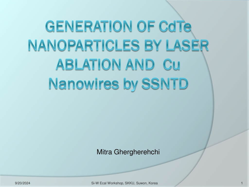
GENERATION OF GENERATION OF C Cd dT Te e NANOPARTICLES BY LASER NANOPARTICLES BY LASER ABLATION AND C ABLATION AND Cu u Nanowires Nanowires by by SSNTD SSNTD Mitra Ghergherehchi 9/20/2024 Si-W Ecal Workshop, SKKU, Suwon, Korea 1
1. Chemical means Collidal route Electrochemical way 2. Physical means Evaporation-condensation method Arc discharge Laser mater interaction( laser ablation) Laser ablation is the process of removing material from a solid (or occasionally liquid) surface by irradiating it with a laser beam. Sub-Picosecond regime, ultra fast laser pulse, Ultra fast plasma laser ablation (UPLA)) Si-W Ecal Workshop, SKKU, Suwon, Korea Nanosecond regime and traditional Laser plasma ablation (long pulse laser) 9/20/2024 2
A 20-TW laser system The gain medium of the laser system is a Ti:sapphire crystal. The minimum pulse duration of the laser system is 31 fs, the maximum energy is 700 mJ. Medical and IT Fusion Research Division, Korea Electrotechnology Research Institute 9/20/2024 Si-W Ecal Workshop, SKKU, Suwon, Korea 3
Semiconductor Materials large active volume high charge carrier motilities high atomic number be operable at room temperature without any cooling apparatus. Good energy resolution requires a relatively small bandgap, 9/20/2024 Si-W Ecal Workshop, SKKU, Suwon, Korea 4
Application solar cells light-emitting diodes in biology Pulsed laser ablation in a liquid media The pulses were focused onto a piece semiconductor, which was held inside a quartz cell with 1 cm pathlength containing 3.5 ml of a solvent of bulk 9/20/2024 Si-W Ecal Workshop, SKKU, Suwon, Korea 5
Solvents and sample preparation (1) acetonitrile, 99.9%); (2) acetone (3) butan-2-ol (4) ethanol (Merck, (5) methanol (6) triethyleneglycol (7) water Bulk CdTe was of cubic structure and consisted of 46.9% Cd and 52.9% 9/20/2024 Si-W Ecal Workshop, SKKU, Suwon, Korea 6
Methods of Nanowires Methods of Nanowires Lithography or Printing on a surface Self Assembly of Nanowires on a surface For instance Writing with tip of Atomic Force Microscopy It Grows wires with few nanometer diameter and less than 10 nm distance directly on a surface Chemical Deposition or Electrodeposition Nanowires can be made of Metals , Semiconductors like Galium Silicon and all kind of polymers It uses a template that can be a nanoporous material that one side is conductor as a working electrod 9/20/2024 Si-W Ecal Workshop, SKKU, Suwon, Korea 7
Some application of nanowires Some application of nanowires Nanowire Materials Applications Advantages Quick respond time Operating at room temperature Pd H2 gas sensor High sensitivity Semiconducting oxides: ZnO, SnO2, and In2O3 CH4, NH3, CO, NOx, O2 gas sensors Works at room temperature (low power) field emitter, heat controlling system High magnetic resistant Cu Online (real time) detection Fast response time Ultra sensitivity High selectivity Ag Explosive and drug sensors Magnetic field sensor, Biomagnetic sensors Bi Giant magneto resistance Online (real time) detection Fast response time High sensitivity Detection of Mecurry in water, Biosensors Au 9/20/2024 Si-W Ecal Workshop, SKKU, Suwon, Korea 8
Techniques and Experiments Ion beam requirements Design and fabrication of ion beam with sufficiently reduced flux density (beam selection) Irradiatedof CR-39 detector with proton chemical etching and surfactant, ion track-etch detector to prepare nanostructures of desired shapes for nano-research Design and fabrication of electrolytic cell nano wire growth with electro depotions method AFM, XRD and SEM observation 9/20/2024 Si-W Ecal Workshop, SKKU, Suwon, Korea 9
Ion beam requirements Proton (Korea Institute of Radiological & Medical Sciences (KIRAMS) Max energy: 30.4 MeV, min energy:15 MeV Current: 1-500 A Beam diameter: 5mm The minimum current intensity is about 1 A (1011#/cm2)which is still too intense. we describe the special requirements for preparing an ion beam with sufficiently reduced flux density( about 104#/cm2) 9/20/2024 Si-W Ecal Workshop, SKKU, Suwon, Korea 10
beam selection 9/20/2024 Si-W Ecal Workshop, SKKU, Suwon, Korea 11
High voltage pulse generator The minimum current intensity is about1 Awhich is still too intense. The irradiation time should be cut into100ns for the purpose of reducing the track density to104cm2. 9/20/2024 Si-W Ecal Workshop, SKKU, Suwon, Korea 12
Magnetic field deflection oAppropriate magnetic field is used for deflecting proton beam 9/20/2024 Si-W Ecal Workshop, SKKU, Suwon, Korea 13
range and energy for CR-39 detectors CR-39 detectors of thickness 1000, 700, 500 m will be vertically irradiate with 20-30MeV proton beam specific energy lose (dE/dx) for CR-39 detector was calculated with SRIM code dE/dx(Kev/ m) 40.74 Proton Energy(Kev) 700 Range 11.22( m) 19.51( m) 1000 32.45 58.85( m) 2000 20.63 115.91( m) 3000 15.20 20000 3.31(mm) 3.34 25000 4.95 (mm) 2.78 30000 6.88(mm) 2.4 9/20/2024 Si-W Ecal Workshop, SKKU, Suwon, Korea 14
Chemical etching and influence of Surfactant Etching co detector in NaOH with appropriate concentration and temperature through the use of surfactant (Sodium Dodecyle Sulfate ) Study the effects of the acid and alkali resistant surfactant (Sodium Dodecyle Sulfate ) on ion track etching at low etch rates and cylindrical pores 9/20/2024 Si-W Ecal Workshop, SKKU, Suwon, Korea 15
Study and calculation the Influence of surfactant concentration on 1- bulk etching rate 2- track etching rate 3- the radial etch rate 4- break through time Study the effects of ultraviolet (UV) irradiation, before etching, on the process of chemical development of ion tracks in CR-39 Find the optimum parameter by controlling the irradiation characteristics, concentration of etchant, surfactant etching time and the 9/20/2024 Si-W Ecal Workshop, SKKU, Suwon, Korea 16
Design and fabrication of electrolytic cell oElectrolytic cell consisting of two identical cell Size of electrolytic cell about few centimeter oMain part of cell in order to etching and electro replication made of PTFE o The metal housing of the cell serves as an electrical shield and acts at the same time as a thermal shield oThe electrodes and filling/flushing tubes are accessible during operation through a slit 9/20/2024 Si-W Ecal Workshop, SKKU, Suwon, Korea 17
Chemical etching in electrolytic cell The first step is the sputter deposition of a gold film on one side of the CR-39 detector Then, the detector that irradiated with proton beam is inserted into an electrolytic cell consisting of two chambers Electrolytic cell used for wire deposition: (1) left chamber, (2) CR-39 detector, (3) Sputtered gold film, (4) copper ring, (5) right chamber 9/20/2024 Si-W Ecal Workshop, SKKU, Suwon, Korea 18
The mechanical stability of the gold film is strengthened by electrodepositing a copper layer in the right cell chamber 9/20/2024 Si-W Ecal Workshop, SKKU, Suwon, Korea 19
The left chamber is filled with the etching solution containing different amounts of NaOH and Surfactant Apply a voltage between a gold wire immersed in the etching solution and the metallic layer deposited on the back of the detector. Measure an electric current as soon as the detector is completely etched through 9/20/2024 Si-W Ecal Workshop, SKKU, Suwon, Korea 20
the data acquisition system The computer controls the data acquisition card, which converts the digital signal from the computer into an analog voltage, which is applied to the conductometric cell. The current through the etched ion track channel is measured and analyzed 9/20/2024 Si-W Ecal Workshop, SKKU, Suwon, Korea 21
Data analysis of electrolytic cell We can obtain with data analysis: current measurement as function of time, track radius as function of time, radial etch rate as function of time, and radial etch rate as function of radius break through time Track and bulk etch rates are determined in real-time If the number of tracks and their length, as well as the conductivity of the etchant is known, the radial etch rate can be determined Stop etching at a preset value of the track diameter by activating an electrical valve 9/20/2024 Si-W Ecal Workshop, SKKU, Suwon, Korea 22
9/20/2024 Si-W Ecal Workshop, SKKU, Suwon, Korea 23
Preparing and manipulating cylindrical micro and nano wires in electrolytic cell After etching CR-39 detector, solution is removed from the cell automatically the chamber is carefully washed with distilled water the chamber is filled with the solution employed for electrodeposition ( in order to copper nano wire growth, Cu2SO4 5H2O and H2SO4). A two-electrode arrangement is used for electrodeposition 9/20/2024 Si-W Ecal Workshop, SKKU, Suwon, Korea 24
The wire is grown at a few hundred -mV potential difference between the two electrodes start nano wire growth The currents during etching and wire growth were measured using a picoammeter When the wire reaches the detector surface, a cap grows on top by analyzing the current recorded during wire growth in a pore, the processing of wire growth correspond to during pore filling, complete pore filling and the beginning of cap growth 9/20/2024 Si-W Ecal Workshop, SKKU, Suwon, Korea 25
Depending concentration of surfactant , applied voltage during the electro deposition and we will be obtained solid wires or hallow wires on properties of detector, etching time, solid wire Hallow wire 9/20/2024 Si-W Ecal Workshop, SKKU, Suwon, Korea 26
After completion of the growth process, the sample is removed from the cell and rinsed with distilled water Dissolving the detector in appropriate solution, wires will be visualized (dichloromethane) 9/20/2024 Si-W Ecal Workshop, SKKU, Suwon, Korea 27
SEM observations Wire shapes resulting from several etchant concentrations and from different etching times were inspected by SEM 9/20/2024 Si-W Ecal Workshop, SKKU, Suwon, Korea 28
XRD observations The preferred growth for the copper nanowires is the direction, which was determined from the XRD pattern 9/20/2024 Si-W Ecal Workshop, SKKU, Suwon, Korea 29
AFM observations With the CS-AFM , I V curves of hundreds of individual copper nanowires will be investigated quickly study behavior of CU nanowires ohm`s law observation 9/20/2024 Si-W Ecal Workshop, SKKU, Suwon, Korea 30
9/20/2024 Si-W Ecal Workshop, SKKU, Suwon, Korea 31