TCAD simulation I
TCAD simulation plays a crucial role in the semiconductor industry, allowing for process and device simulations to meet market demands and reduce development time and costs. This involves modeling transport regimes, semiconductor equations, and electromagnetic fields to drive charge flow self-consis
1 views • 29 slides

Statistical Interpretation of Life Test
This presentation delves into the comparison between MIL and JEDEC requirements for semiconductor life tests, focusing on JEP001-1A, 2A, and 3A guidelines. It explores the significance of life test data, what it can demonstrate for reliability, and the importance of volume in testing. The content di
0 views • 21 slides

Florida Statewide Assessments - Summer 2023 Overview
Training materials for the Summer 2023 Florida Statewide Assessments in Miami-Dade County Public Schools, focusing on test administration policies and procedures. The materials are based on the Spring/Summer 2023 Test Administration Manual and cover important information related to test administrati
0 views • 69 slides
Exploring Growth Opportunities in Small Semiconductor Equipment Companies
Dive into the transformation of the semiconductor equipment industry from cyclical to growth-driven, backed by data from world semiconductor trade statistics, and insights from companies like Taiwan Semiconductor (TSM). Discover the increasing complexity in semiconductor packaging techniques and how
4 views • 41 slides

Module C1:Material substitution.
Explore the concept of material substitution in the context of circular economy principles for energy storage. Understand the importance of material availability, limitations of secondary raw materials in energy applications, and classification of energy conversion and supportive materials. Discover
5 views • 16 slides
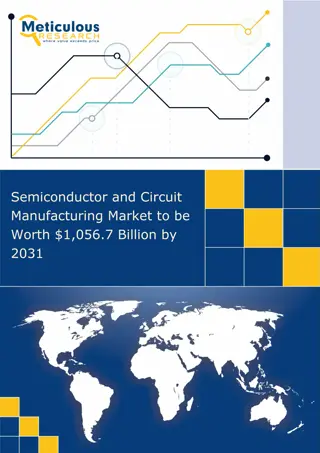
Semiconductor and Circuit Manufacturing Market
Semiconductor and Circuit Manufacturing Market by Component (Memory, Logic, Analog, Micro), Semiconductor (Intrinsic, Extrinsic), Material (Silicon, Germanium), Application (Consumer, Automotive, Industrial), & Geography - Global Forecast to 2031.
1 views • 5 slides
Comprehensive Industrial Wood Construction Education Materials for 2022
Extensive teaching materials for industrial wood construction education in 2022, prepared by various educational institutions and industry experts. The materials cover topics such as construction economy, project management, and specialized knowledge on wood construction. Students will gain insights
1 views • 32 slides

Diamond Semiconductor Substrates Market Outlook, Growth Driver
Adroit Market Research has included the Global Diamond Semiconductor Substrates Market\u00a0research to its database in order to provide a thorough analysis of the variables driving a general market growth trend.
0 views • 5 slides

Significance of Raw Materials in Food Processing
Effective selection of raw materials is crucial for ensuring the quality of processed food products. The quality of raw materials directly impacts the final products, making it important to procure materials that align closely with processing requirements. Quality evaluation, including microbiologic
2 views • 30 slides

Understanding Semiconductor Sensors and their Applications
Semiconductor sensors are versatile devices that utilize semiconductor materials like silicon for detecting and measuring various non-electrical quantities. These sensors leverage the unique properties of silicon, such as high tensile strength, Young Modulus, and resistance to corrosion, making them
1 views • 26 slides
Overview of Semiconductor Materials and Applications
Understanding electronic transport in semiconductors is essential for various applications such as computers, smartphones, LEDs, and more. Semiconductors like silicon and compound semiconductors play a crucial role in creating devices with unique properties. By delving into the world of semiconducti
0 views • 20 slides

Understanding Dental Impression Materials and Techniques
Dental impression materials are essential in dentistry to create precise negative records of the oral tissues. The process involves obtaining a negative impression and then producing a positive reproduction using materials like dental stone. These materials must meet specific desirable properties to
1 views • 18 slides
Understanding Composite Materials: Properties and Applications
Composite materials are combinations of chemically distinct substances that offer improved properties over individual materials. They can be natural or synthetic, with examples like wood and bamboo. Composites consist of reinforcing fibers or particles embedded in a matrix material. Smart materials,
1 views • 9 slides

Understanding P-N Junction and Semiconductor Physics
A p-n junction is a crucial interface in semiconductor devices that consists of a p-type and an n-type material, creating a boundary with distinctive charge carriers. By doping different semiconductor materials, a p-n junction can be formed, enabling the diffusion and drift of electrons and holes ac
0 views • 25 slides

Understanding the Importance and Methods of Materials Testing
Ensuring materials in infrastructure and equipment meet performance standards is crucial for sustainable production. Materials testing, encompassing destructive and non-destructive methods, provides valuable insights into material properties. From tensile to compression tests, understanding stress a
2 views • 28 slides
Understanding Thermal Properties of Materials
Materials respond differently to heat based on their thermal properties such as heat capacity, thermal expansion, conductivity, and shock resistance. The ability of materials to absorb heat, expand with temperature changes, and conduct heat varies across ceramics, metals, and polymers. Heat capacity
0 views • 19 slides
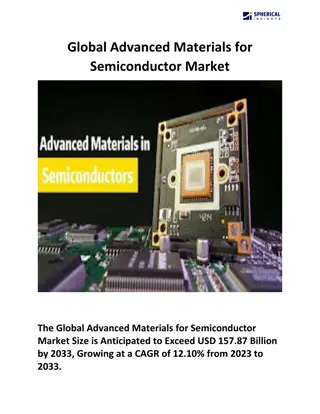
Global Advanced Materials for Semiconductor Market
\"The Global Advanced Materials for Semiconductor Market Size is Anticipated to Exceed USD 157.87 Billion by 2033, Growing at a CAGR of 12.10% from 2023 to 2033.\n\"\n
0 views • 5 slides
Understanding Physical Properties of Materials in Grade 7 Natural Sciences
Exploring the physical properties of materials like strength and flexibility helps us decide which materials to use for specific purposes. Strong materials like steel and concrete are used in construction, while flexible materials like rubber and copper wire have different applications. Consideratio
1 views • 17 slides
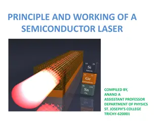
Understanding the Principle and Working of Semiconductor Lasers
Semiconductor lasers operate through absorption, spontaneous emission, and stimulated emission processes. Absorption of radiation causes electrons to jump to higher energy levels, leading to light emission. Spontaneous emission is when excited electrons return to ground state by emitting photons, wh
3 views • 17 slides
Understanding Schottky Diodes in Electronics
The Schottky diode is a semiconductor device known for its low forward voltage drop and fast switching action. Unlike ordinary diodes, it forms a metal-semiconductor junction, resulting in higher efficiency and faster switching speeds. This article explores the construction, working principle, and k
4 views • 11 slides

Understanding Impact Testing for Materials Evaluation
Impact testing is crucial for assessing the toughness and resistance of materials to fracture under high-rate loading conditions. Charpy and Izod tests are common methods used to measure impact energy and evaluate materials' performance. The tests involve striking a specimen with a striker and measu
2 views • 13 slides
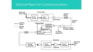
Overview of Point-to-Point Fiber Optic Communication System
Point-to-point fiber optic communication systems involve converting voice signals from a microphone into digital signals using a coder, transmitting light signals through a semiconductor diode laser over optical fibers, and decoding the signals back to analog for sound production. The system offers
0 views • 11 slides

Understanding Quaternaries in Semiconductor Nanodevice Design
Learn about the treatment of quaternary materials in semiconductor nanodevice simulations, including material parameters needed for GaAs/AlGaAs heterostructures and interpolation techniques for ternaries. Explore the complexities of AlxGa1-xAsyP1-y and AlxGa1-xIn1-x-yAs quaternaries, along with the
0 views • 10 slides
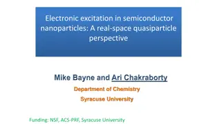
Understanding Electronic Excitation in Semiconductor Nanoparticles from a Real-Space Quasiparticle Perspective
This research delves into the electronic excitation in semiconductor nanoparticles, focusing on real-space quasiparticle perspectives. It explores treating electron correlation using explicit operators, leading to faster algorithms while calculating optical gap and exciton binding energies. Various
0 views • 45 slides

Materials Science: Revolutionizing Innovation in the Next Decade
Materials science is poised to be the cornerstone of technological advancements in the next decade, addressing challenges such as clean energy, product innovation, and material supply disruptions. Scientists are leveraging advanced simulation techniques and machine learning to accelerate materials r
2 views • 15 slides
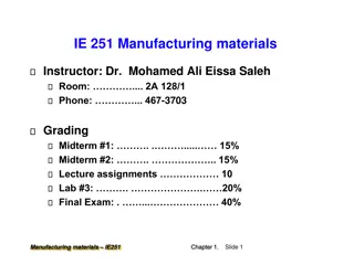
IE 251 Manufacturing Materials Course Overview
Explore the impact of modern materials on daily products, understand engineering materials and their properties, and delve into classes of materials like metals, polymers, ceramics, and composites. The course covers topics ranging from atomic structure to phase transformations, emphasizing the role
0 views • 14 slides
Understanding Materials Science and Engineering Fundamentals
Materials play a crucial role in our daily lives, influencing everything from transportation to communication. This lecture delves into the historical significance of materials, the distinctions between materials science and materials engineering, and the importance of structure-property correlation
0 views • 25 slides
Exploring Materials in Everyday Objects
Discover the suitability of different materials for specific uses through fun activities like a spoon race with various spoon materials. Explore why certain materials are not appropriate for certain objects and engage in creative tasks like imagining a spoon made of tissue paper. Michael Rosen's whi
0 views • 6 slides
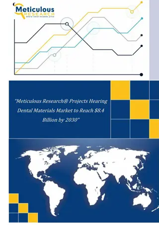
Dental Materials Market
The dental materials market is categorized based on type\u2014comprising Indirect Restorative Materials (metal-ceramics, ceramics, and other indirect materials), Direct Restorative Materials (amalgam, resin-based composites, glass ionomer, and other
0 views • 4 slides

Managing E-Beam Drift for Semiconductor Fabrication
Explore techniques to address e-beam drift issues in semiconductor manufacturing, such as alignment using wafer marks and multi-pass writing strategies. Learn how to minimize drift problems and improve productivity in the fabrication process.
0 views • 44 slides

Understanding PN Junction in Semiconductors
Mobility in semiconductors is affected by scattering events as temperature increases, with impurity scattering dominating at low temperatures and lattice scattering at high temperatures. A p-n junction is the interface between p-type and n-type semiconductor materials, with excess holes on the p-sid
0 views • 15 slides
Understanding Extrinsic Semiconductors: Fermi Level and Doping Effects
Extrinsic semiconductors play a crucial role in modern electronics by allowing controlled addition of impurities to tailor conductivity. The Fermi level in extrinsic semiconductors shifts based on the number of electrons and holes in the conduction and valence bands, influencing conductivity. Doping
0 views • 14 slides

Understanding Raw Materials in Ceramic Production
Raw materials play a crucial role in ceramic production, with three main groups identified - plastic materials like clay, non-plastic or leading mixtures such as silica, and fluxes/mineralizers like feldspar. These materials undergo various transformations during the manufacturing process, contribut
0 views • 29 slides

Comprehensive Overview of Full Ceramic Grid Technology in Microfabrication
Explore the innovative full ceramic grid technology in microfabrication, including insights into the process flow, materials utilized, and applications. Learn about the components, layers, and bonding techniques involved in this advanced manufacturing method, offering high precision and thermal stab
0 views • 12 slides
Understanding Semiconductor Conductivity and Scattering Mechanisms
In the study of semiconductor conductivity, the concept of degenerate and non-degenerate semiconductors is discussed, showcasing the impact of doping levels. The conductivity equation is explored in terms of electron and hole mobilities and densities. The role of scattering mechanisms, such as latti
0 views • 18 slides
Plasma Etching Challenges and Solutions in Semiconductor Fabrication
Understanding the importance of plasma etching in semiconductor fabrication, this discourse delves into the challenges faced in modeling modern etch processes. Topics covered include stochastic defect detection, reactor-level plasma physics, and an integrated model hierarchy approach. Techniques suc
0 views • 14 slides
Emerging Materials for MOS-Transistor Gate Stacks in Semiconductor Technology
Advancements in semiconductor technology necessitate the adoption of new materials for gate stacks in MOS-transistors, addressing issues like gate leakage current and gate oxide problems. With the continual scaling down of MOSFETs, the use of high-K materials offers solutions to enhance performance
0 views • 51 slides
Laser Ablation for Generation of Nanoparticles and Nanowires: Workshop Insights
Explore the latest research on laser ablation techniques for generating nanoparticles and nanowires, presented at the Si-W Ecal Workshop in Korea. Discover the various methods, applications in solar cells and LEDs, and the use of semiconductor materials. Learn about the advanced 20-TW laser system a
0 views • 31 slides

Understanding Double Patterning Lithography Techniques
Explore the world of lithography with a focus on double patterning techniques. From self-aligned double patterning to chemical vapor deposition methods, this comprehensive overview covers the key concepts, challenges, and solutions in advanced semiconductor manufacturing processes. Dive into the int
0 views • 28 slides