Understanding the Impact of Temperature on Fermi Level in Semiconductors
The Fermi level plays a crucial role in determining the behavior of electrons in semiconductors at different temperatures. As temperature increases, the Fermi level shifts, affecting the generation of free electrons and holes in the valence and conduction bands. In intrinsic semiconductors, electron and hole concentrations are equal, while in extrinsic semiconductors, they differ due to added impurities. This shift in Fermi level influences the probability of energy level occupation and the behavior of n-type and p-type semiconductors, leading to distinct characteristics in conduction and valence bands.
Download Presentation

Please find below an Image/Link to download the presentation.
The content on the website is provided AS IS for your information and personal use only. It may not be sold, licensed, or shared on other websites without obtaining consent from the author. Download presentation by click this link. If you encounter any issues during the download, it is possible that the publisher has removed the file from their server.
E N D
Presentation Transcript
EFFECT OF TEMPERATURE IN FERMI LEVEL DR.A.ANBARASI ASSOCIATE PROFESSOR IN PHYSICS PERIYAR ARTS COLLEGE CUDDALORE
The probability of occupation of energy levels in valance and conduction band is represented in terms of Fermi level. As the temperature increases, free electrons and holes gets generated which results in shift of Fermi level accordingly. In intrinsic semiconductor, the no. of electrons in conduction band and no. of holes in valance band are equal. The probability of occupation of energy levels in valance and conduction band are equal.
FERMI LEVEL OF INTRINSIC SEMICONDUCTOR Hence, the Fermi level for intrinsic semi conductor lies in the middle of the forbidden band. In extrinsic semiconductor, the no. of electrons in conduction band and no. of holes in valance band are not equal. Fermi level in n-type semiconductor In n-type semiconductor, pentavalent impurity is added which donates a free electron. This creates large no. of free electrons in conduction band. At room temperature, no. of electrons in conduction band are greater than no. of holes in valance band. The probability of occupation of energy levels by electrons in conduction band is greater than that of holes in the valance band.
FERMI LEVEL OF SEMICONDUCTORS Therefore, the Fermi level in n-type lies closer to the conduction band. As the temperature increases, the Fermi level shifts towards the conduction band. Fermi level in p-type semiconductor In p-type semiconductor, trivalent impurity is added which creates hole in valance band and is ready to accept an electron. This creates large no. of holes in the valance band. At room temperature, the no. of holes in the valance band are greater than the no. of electrons in conduction band. The probability of occupation of energy levels by holes in valance band is greater than that of the electrons in conduction band.
TEMPERATURE INCREASES FERMI LEVEL SHIFTS Therefore, the Fermi level for p-type lies closer to the valance band. As the temperature increases, the Fermi level for p-type shifts towards the valance band.
FERMI LEVEL AND ITS CHANGES The Fermi level lies between the valence band and conduction band because at absolute zero temperature the electrons are all in the lowest energy state. ... The Fermi level changes as the solids are warmed and as electrons are added to or withdrawn from the solid.
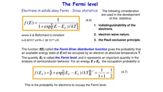
FERMI LEVEL CHANGES WITH TEMPERATURE Does Fermi energy depend on temperature? The experiment shows that the Fermi level decreases with increasing temperature and has almost the same temperature dependence as the energy gap. It is pinned at about 0.63 of energy gap below the conduction band.
FERMI ENERGY What is the formula of Fermi energy? Fermi Energies for Metals We can also turn this around and express the Fermi energy in terms of the free electron density. For a metal with Fermi energy EF= eV, the free electron density is n = x10^ electrons/m3.
FERMI LEVEL What do you understand by Fermi level? The Fermi Level is the energy level which is occupied by the electron orbital at temperature equals 0 K. The level of occupancy determines the conductivity of different materials This Photo by Unknown Author is licensed under CC BY-SA
What is the Fermi radius? In reciprocal space, the Fermi surface of an ideal Fermi gas is a sphere of radius. , determined by the valence electron concentration where. is the reduced Planck's constant. A material whose Fermi level falls in a gap between bands is an insulator or semiconductor depending on the size of the bandgap This Photo by Unknown Author is licensed under CC BY-SA
Is Fermi energy constant? The value of the Fermi level at absolute zero temperature ( 273.15 C) is known as the Fermi energy. It is also the maximum kinetic energy an electron can attain at 0K.Fermi energy is constant for each solid.
ENERGY SPECTRUM What are the factors on which Fermi energy depends? the nature and concentration of the impurity in the semiconductor; 2. the temperature. These two factors make the Fermi level moveable within the energy spectrum.
SILICON & GERMANIUM Which is better silicon or germanium? The structure of Germanium crystals will be destroyed at higher temperature. However,Silicon crystals are not easily damaged by excess heat. Peak Inverse Voltage ratings of Silicon diodes are greater than Germanium diodes. Si is less expensive due to the greater abundance of element.
TAUC PLOT How is band gap measured? The direct optical band gap of semiconductors is traditionally measured by extrapolating the linear region of the square of the absorption curve to the x-axis, and a variation of this method, developed by Tauc, has also been widely used.
FERMI PRESSURE What is Fermi pressure? The Pauli exclusion principle disallows two identical half-integer spin particles (electrons and all other fermions) from simultaneously occupying the same quantum state. ... The result is an emergent pressure against compression of matter into smaller volumes of space.
WHY DO ELECTRONS MOVE FASTER THAN HOLES? As electrons are of lighter mass than holes so their acceleration are more than that of holes which follow drift velocity inside conductor,making electron move much faster.
TUNNEL DIODE A tunnel diode (also known as a Esaki diode) is a type of semiconductor diode that has effectively negative resistance due to the quantum mechanical effect called tunneling.Tunnel diodes have a heavily doped pn junction that is about 10 nm wide.
A tunnel diode or Esaki diode is a type of semiconductor diode that has effectively "negative resistance" due to the quantum mechanical effect called tunneling. It was invented in August 1957 by Leo Esaki, Yuriko Kurose, and Takashi Suzuki when they were working at Tokyo Tsushin Kogyo, .
Tunnel Diode is the P-N junction device that exhibits negative resistance. When the voltage is increased than the current flowing through it decreases. It works on the principle of the Tunneling effect.
A Tunnel diode is a heavily doped p-n junction diode in which the electric current decreases as the voltage increases. In tunnel diode, electric current is caused by Tunneling . The tunnel diode is used as a very fast switching device in computers. It is also used in high-frequency oscillators and amplifiers.
What is tunnel diode and its working? A Tunnel Diode is a heavily doped p-n junction diode. The tunnel diode shows negative resistance. When voltage value increases, current flow decreases. Tunnel diode works based on Tunnel Effect. ... Therefore, it is also called as Esaki diode.
How tunnel diode is used as oscillator? The oscillator circuit that is built using a tunnel diode is called as a Tunnel diode oscillator. If the impurity concentration of a normal PN junction is highly increased, this Tunnel diode is formed. It is also known as Esaki diode, after its inventor.
What is the difference between zener diode and tunnel diode? A zener diode is used for voltage regulation. ... The zener is used for voltage reference, as well as to limit certain voltages where 1 or 2 diodes would not provide the needed voltage level for a circuit. The Tunnel diode can be used as an amplifier, or usually as an oscillator, but it can also be used as a switch.
What is diode and its types? An Overview on Different Types of Diodes and Their Uses. A diode is a two-terminal electrical device, that allows the transfer of current in only one direction. The diode is also known for its unidirectional current property, where the electric current is permitted to flow in one direction.
SEMICONDUCTOR OBJECTIVE TYPE QUESTIONS AND ANSWERS Q1. A semiconductor is formed by bonds. Covalent Electrovalent Co-ordinate None of the above Answer : 1
Q2. A semiconductor has temperature coefficient of resistance. Positive Zero Negative None of the above Answer : 3
Q3 The most commonly used semiconductor is .. Germanium Silicon Carbon Sulphur Answer : 2
Q4. A semiconductor has generally valence electrons. 1.2 2.3 3.6 4.4 Answer : 4
5. The resistivity of pure germanium under standard conditions is about . 6 x 104 cm 60 cm 3 x 106 cm 6 x 10⁻⁴ cm Answer :.52 ohm
6. The resistivity of a pure silicon is about 100 cm 6000 cm 3 x 10⁵ m 6 x 10⁻⁸ cm Answer : 2
7. When a pure semiconductor is heated, its resistance .. Goes up Goes down Remains the same Can t say Answer : 2
9)The strength of a semiconductor crystal comes from .. Forces between nuclei Forces between protons Electron-pair bonds None of the above Answer : 3
Q10. Addition of pentavalent impurity to a semiconductor creates many .. Free electrons Holes Valence electrons Bound electrons Answer : 1
Q11. A pentavalent impurity has . Valence electrons 3 5 4 6 Answer : 2
Q.12. An n-type semiconductor is Positively charged Negatively charged Electrically neutral None of the above Answer : 3
Q13. A trivalent impurity has .. valence electrons 4 5 6 3 Answer : 4
Q14. Addition of trivalent impurity to a semiconductor creates many .. Holes Free electrons Valence electrons Bound electrons Answer : 1
Q15. A hole in a semiconductor is defined as . A free electron The incomplete part of an electron pair bond A free proton A free neutron Answer : 2
Q16. The impurity level in an extrinsic semiconductor is about .. of pure semiconductor. 10 atoms for 108atoms 1 atom for 108atoms 1 atom for 104atoms 1 atom for 100 atoms Answer : 2
Q17. As the doping to a pure semiconductor increases, the bulk resistance of the semiconductor .. Remains the same Increases Decreases None of the above Answer : 3
Q18. A hole and electron in close proximity would tend to . Repel each other Attract each other Have no effect on each other None of the above Answer : 2
Q19. In a semiconductor, current conduction is due to .. Only holes Only free electrons Holes and free electrons None of the above Answer : 3
Q20. The random motion of holes and free electrons due to thermal agitation is called . Diffusion Pressure Ionisation None of the above Answer : 1
Q21. A forward biased pn junction diode has a resistance of the order of k M None of the above Answer : 1
Q22. The battery connections required to forward bias a pn junction are +ve terminal to p and ve terminal to n -ve terminal to p and +ve terminal to n -ve terminal to p and ve terminal to n None of the above Answer : 1
Q23. The barrier voltage at a pn junction for germanium is about 5 V 3 V Zero 3 V Answer : 4


