Exploring Diode and Transistor Logic Circuits for LED Blinking and Logic Operations
Dive into the world of diode and transistor logic circuits with designs for NAND and AND gates, as well as LED blinking circuits using stable multi-vibrators. Learn how these circuits function and discover the components involved in creating a square wave generator. Explore the practical applications of these circuits in real-time scenarios like police lights and emergency vehicle lights.
- Diode Logic Circuits
- Transistor Logic Circuits
- LED Blinking Circuit
- Square Wave Generator
- Real-Time Applications

Download Presentation

Please find below an Image/Link to download the presentation.
The content on the website is provided AS IS for your information and personal use only. It may not be sold, licensed, or shared on other websites without obtaining consent from the author. Download presentation by click this link. If you encounter any issues during the download, it is possible that the publisher has removed the file from their server.
E N D
Presentation Transcript
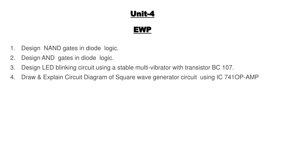
Unit Unit- -4 4 EWP EWP 1. 2. 3. 4. Design NAND gates in diode logic. Design AND gates in diode logic. Design LED blinking circuit using a stable multi-vibrator with transistor BC 107. Draw & Explain Circuit Diagram of Square wave generator circuit using IC 741OP-AMP
AND Gate AND Gate using diode logic using diode logic
AND Gate AND Gate using diode logic using diode logic When X = +5 V and Y= + 5 V, both diodes D1 and D2 are reverse biased (O.C.). No current will flow through resistor R and no voltage drop across resistor R. Hence output across O.C. is maximum so Z=+5 V. When X=0 or Y=0 or both X=Y=0 volt, either diode D1 or D2 or both D1 and D2 are forward biased (S.C.). Entire current will flow through resistor R. So output across S.C. is zero and hence Z = 0 V.
N NAND Gate AND Gate using diode & Transistor logic using diode & Transistor logic When A=+5 V and B=+5 V, both diodes are reverse baised (O.C.). So current will flow through resistor R2 and transistor Q1 gets enough base deive from suppy thorugh R2 and hence Q1 switch is ON and output X=Vce= 0 V. When A=0 V or B=0 V or both A=B=0 v, transistor Q1 is OFF and output X= +5 V.
Design LED blinking circuit using a stable multi Design LED blinking circuit using a stable multi- -vibrator with transistor BC 107. transistor BC 107. vibrator with Real time application Timer Module Police Light Emergency vehicle Light
Design LED blinking circuit using a stable multi Design LED blinking circuit using a stable multi- -vibrator with transistor BC 107. transistor BC 107. vibrator with This circuit generate two different not stabled state outputs pulses. We can connect the LED in the two output pulse point and our LED blink easily. When the supply is swithced ON, capacitors C1 and C2 charge at the same time. That time LED1 and LED2 are in OFF condition. When C1 or C2 gets charged fully, any of the capacitor discharges the charged power. That time cross coupled transistor get active and acts like a switch (ON mode), and connect the ground line to LED cathode side and hence the corresponding LED turns ON. Once discharged completely, that capacitor goes to charge. At that time parallel capacitor discharges. So another LED will be turned ON. This process continuously doing so LED will be blink. You can change the blink time by change the capacitor C1, C2 values.
Circuit Diagram of Square wave generator circuit using IC Circuit Diagram of Square wave generator circuit using IC 741 OP 741 OP- -AMP AMP
M Multivibrator circuit ultivibrator circuit A multivibrator circuit oscillates between a HIGH state and a LOW state producing a continuous output. Astable A free-running multivibrator that has NO stable states but switches continuously between two states this action produces a train of square wave pulses at a fixed known frequency. Monostable A one-shot multivibrator that has only ONE stable state as once externally triggered it returns back to its first stable state. Bistable A flip-flop that has TWO stable states producing a single pulse either HIGH or LOW in value. In the circuit diagram capacitor C1 and potentiometer R1 forms the timing part. Resistors R2 and R3 forms a voltage divider network which supplies a fixed fraction of the output voltage into the non-inverting pin of the OP-AMP as a reference voltage.
Working Working Initially the voltage across the capacitor C1 will be zero and the output of the opamp will be high. As a result the capacitor C1 starts charging to positive voltage through potentiometer R1. When the C1 is charged to a level so that the voltage at the inverting terminal of the opamp is above the voltage at the non-inverting terminal, the output of the opamp swings to negative. The capacitor quickly discharges through R1 and then starts charging to negative voltage. When the C1 is charged to a negative voltage so that the voltage at the inverting input more negative than that of the non-inverting pin, the output of the opamp swings back to positive voltage. Now the capacitor quickly discharges the negative voltage through R1 and starts charging to positive voltage. This cycle is repeated endlessly and the result will a continuous square wave swinging between +Vcc and -Vcc at the output. The common practice is to make the R3 equal to R2. Then the equation for the time period can be simplified as: T=2.1976R1C1