Understanding Bipolar Transistor Configurations for Electronic Circuits
Explore the three common configurations - Common Base, Common Emitter, and Common Collector - for Bipolar Transistors in electronic circuits. Each configuration offers unique characteristics such as voltage gain, current gain, and impedance levels, impacting the signal processing and amplification capabilities. Learn about the application scenarios and benefits of each configuration to design efficient transistor-based circuits.

Download Presentation

Please find below an Image/Link to download the presentation.
The content on the website is provided AS IS for your information and personal use only. It may not be sold, licensed, or shared on other websites without obtaining consent from the author. Download presentation by click this link. If you encounter any issues during the download, it is possible that the publisher has removed the file from their server.
E N D
Presentation Transcript
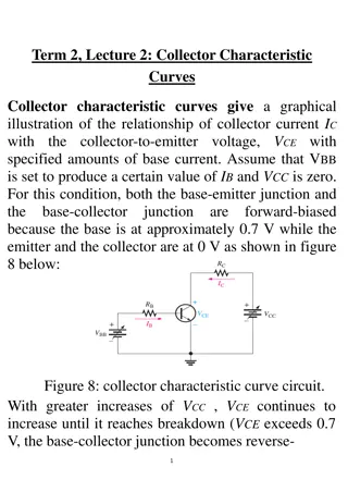
Transistors Dr.Kadry Ali Ezzat
Bipolar Transistor Configurations As the Bipolar Transistor is a three terminal device, there are basically three possible ways to connect it within an electronic circuit with one terminal being common to both the input and output. Each method of connection responding differently to its input signal within a circuit as the static characteristics of the transistor vary with each circuit arrangement. Common Base Configuration has Voltage Gain but no Current Gain. Common Emitter Configuration has both Current and Voltage Gain. Common Collector Configuration has Current Gain but no Voltage Gain.
The Common Base (CB) Configuration As its name suggests, in the Common Base or grounded base configuration, the BASE connection is common to both the input signal AND the output signal. The input signal is applied between the transistors base and the emitter terminals, while the corresponding output signal is taken from between the base and the collector terminals as shown. The base terminal is grounded or can be connected to some fixed reference voltage point. The input current flowing into the emitter is quite large as its the sum of both the base current and collector current respectively therefore, the collector current output is less than the emitter current input resulting in a current gain for this type of circuit of 1 (unity) or less, in other words the common base configuration attenuates the input signal.
Common Base Voltage Gain Where: Ic/Ie is the current gain, alpha ( ) and RL/Rin is the resistance gain. The common base circuit is generally only used in single stage amplifier circuits such as microphone pre-amplifier or radio frequency ( R ) amplifiers due to its very good high frequency response.
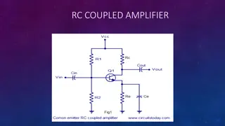
The Common Emitter (CE) Configuration In the Common Emitter or grounded emitter configuration, the input signal is applied between the base and the emitter, while the output is taken from between the collector and the emitter as shown. This type of configuration is the most commonly used circuit for transistor based amplifiers and which represents the normal method of bipolar transistor connection. The common emitter amplifier configuration produces the highest current and power gain of all the three bipolar transistor configurations. This is mainly because the input impedance is LOW as it is connected to a forward biased PN-junction, while the output impedance is HIGH as it is taken from a reverse biased PN- junction.
In this type of configuration, the current flowing out of the transistor must be equal to the currents flowing into the transistor as the emitter current is given as Ie = Ic + Ib. As the load resistance ( RL) is connected in series with the collector, the current gain of the common emitter transistor configuration is quite large as it is the ratio of Ic/Ib. A transistors current gain is given the Greek symbol of Beta, ( ). As the emitter current for a common emitter configuration is defined as Ie = Ic + Ib, the ratio of Ic/Ie is called Alpha, given the Greek symbol of . Note: that the value of Alpha will always be less than unity. Then, small changes in current flowing in the base will thus control the current in the emitter-collector circuit. Typically, Beta has a value between 20 and 200 for most general purpose transistors. So if a transistor has a Beta value of say 100, then one electron will flow from the base terminal for every 100 electrons flowing between the emitter-collector terminal.
The Common Collector (CC) Configuration In the Common Collector or grounded collector configuration, the collector is now common through the supply. The input signal is connected directly to the base, while the output is taken from the emitter load as shown. This type of configuration is commonly known as a Voltage Follower or Emitter Follower circuit. The common collector, or emitter follower configuration is very useful for impedance matching applications because of the very high input impedance, in the region of hundreds of thousands of Ohms while having a relatively low output impedance.
BJT Operating Regions Operating Region Parameters Mode VBE < (Vcut-in =0.7v) VCE > Vsupply IB = IC = 0 Cut Off Switch OFF VBE >= (Vcut-in =0.7v) Vsat < VCE < Vsupply IC = *IB Ib > 0, and Ic > 0 Amplificati on Linear VBE >= (Vcut-in =0.7v) VCE <= Vsat =0.2 v IB> IC,max, IC,max > 0 Ib > 0, and Ic > 0 Saturated Switch ON
BJT Applications BJT Switch Offer lower cost and substantial reliability over conventional mechanical relays. Transistor operates purely in a saturated or cutoff state (on/off) This can prove very useful for digital applications (small current controls a larger current)
BJT Applications BJT Amplifier
BJT Characteristic Curves Transfer Characteristic Characteristic curves can be drawn to show other useful parameters of the transistor The slope of ICE/ IBE is called the Transfer Characteristic ( )
BJT Characteristic Curves Input Characteristic The Input Characteristic is the base emitter current IBEagainst base emitter voltage VBE IBE/VBE shows the input Conductance of the transistor. The increase in slope of when the VBEis above 1 volt shows that the input conductance is rising There is a large increase in current for a very small increase in VBE.
BJT Characteristic Curves Output Characteristic collector current (IC) is nearly independent of the collector-emitter voltage (VCE), and instead depends on the base current (IB) IB4 IB3 IB2 IB1
BJT Applications BJT Amplifier


 Configuration")
 Configuration")

 Configuration")
 Configuration")


 Configuration")
 Configuration")
 Configuration")
 Configuration")